PCB Manufacturing
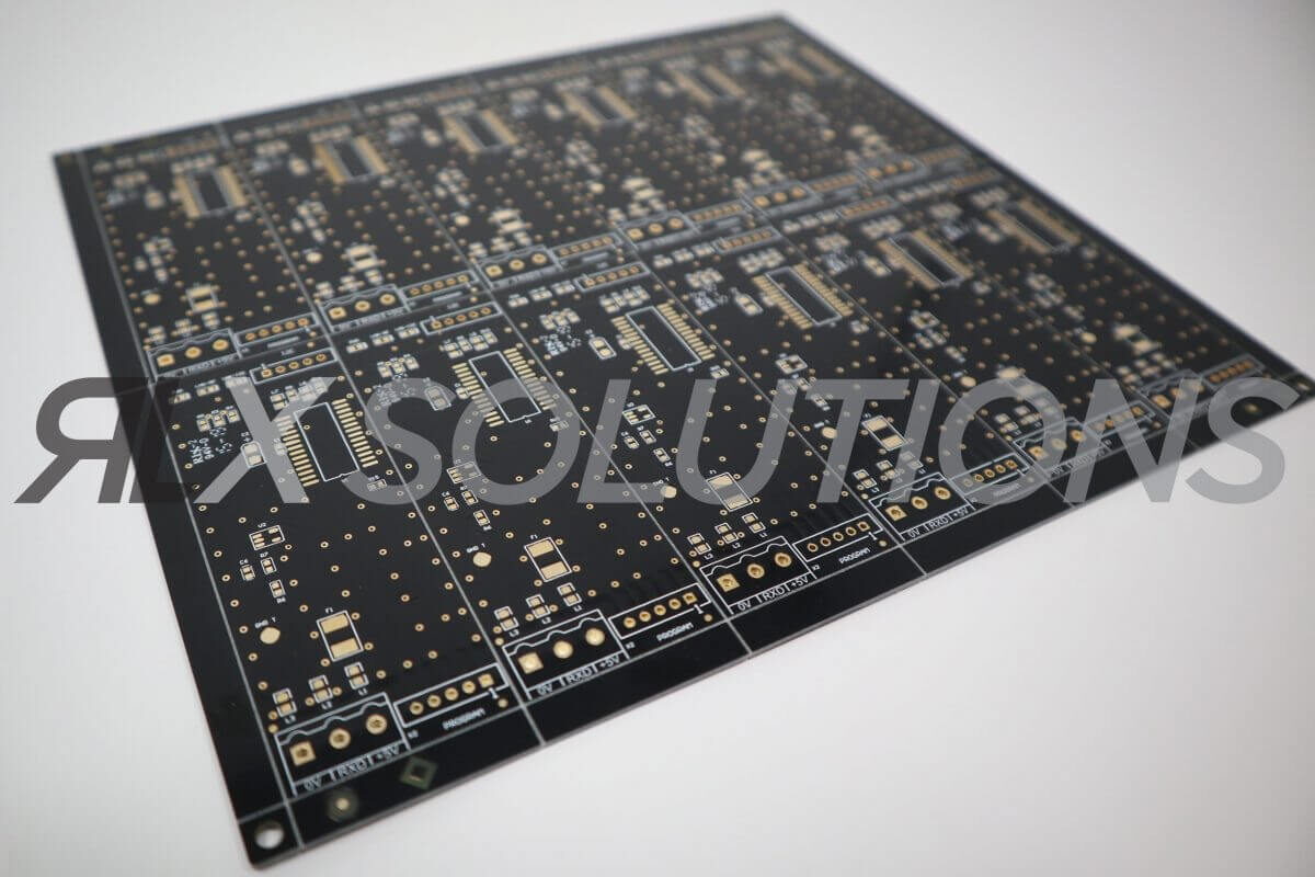
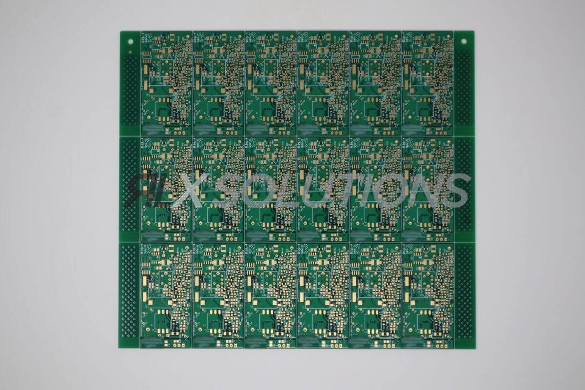
Bare PCB fabrication — FR-4, high-Tg, halogen-free, aluminum MCPCB, rigid-flex, polyimide, HDI, high-frequency. 1–24 layers standard.
View capabilities →RLX Solutions is a Canadian electronics manufacturer offering PCB fabrication, turnkey assembly, component procurement, custom cable and harness assembly, LED products, and engineering support. Incorporated in 2013, we're UL listed, ISO 9001:2015 certified, and built for regulated-industry work. One quote, one program manager, from prototype through sustained production.
We match the capability depth of large overseas prototype houses and pair it with Canadian-registered quality systems, real DFM review, and a supply chain your procurement team can audit.
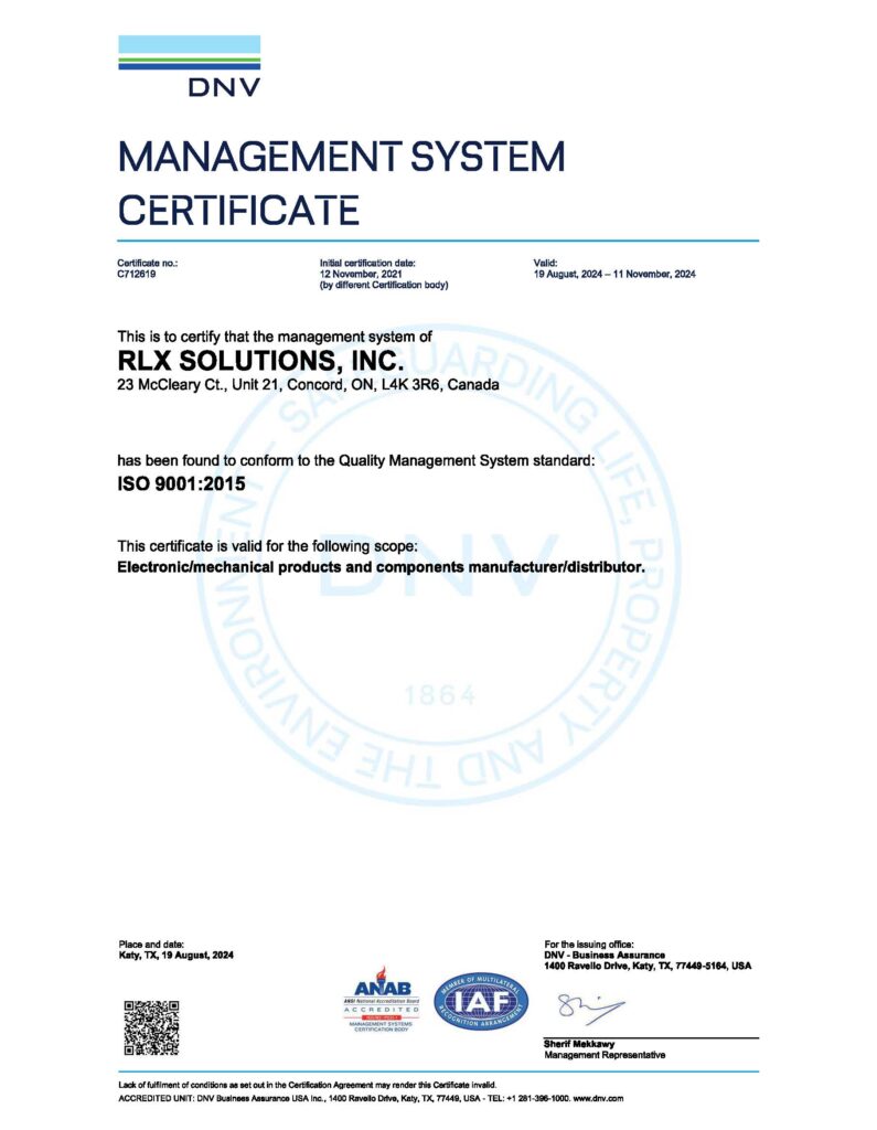
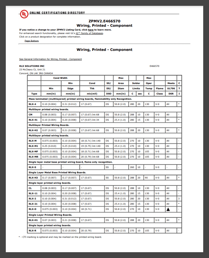
UL #E466570 since 2013. ISO certificate #C712619 issued by DNV. IPC-A-610 Class 2 and Class 3 workmanship. Documents published on request.
Blind & buried vias, HDI microvias, rigid-flex, metal-core, controlled impedance, 01005 passives, 0.3 mm BGA pitch. See the capability reference below for the full envelope.
Every quote gets a real DFM / DFA review before fabrication. No automated rubber-stamp, no wait for offshore clarification. Included, not extra.
Authorized distribution plus verified excess-inventory sourcing for obsolete and allocated parts. Full lot and date-code traceability.
The standard envelope of every service we offer, organized the way an engineer evaluates a manufacturer: PCB parameters, drilling, traces, via types, surface finishes, impedance, special processes, and test. Specs are our routine production envelope. Anything beyond — 28-layer stackups, sub-2 mil traces, copper in >6 oz, controlled impedance tighter than ±5% — is available on request. Ask.
Pick the process you need from the tabs. Check your design against the specs. If your file passes, it's a routine build. If it doesn't, tell us what's off — 90% of edge cases are builds we quote without issue.
Standard FR-4, high-Tg, halogen-free · CEM-1 / CEM-3 on request · panelized for volume SMT
Matte black soldermask with ENIG gold-plated pads · fine-pitch BGA ready · premium aesthetic
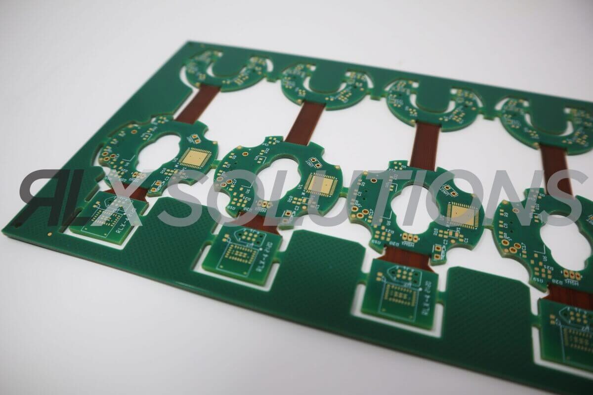
Polyimide flex up to 8 layers · rigid-flex up to 12 layers total · bookbinder construction
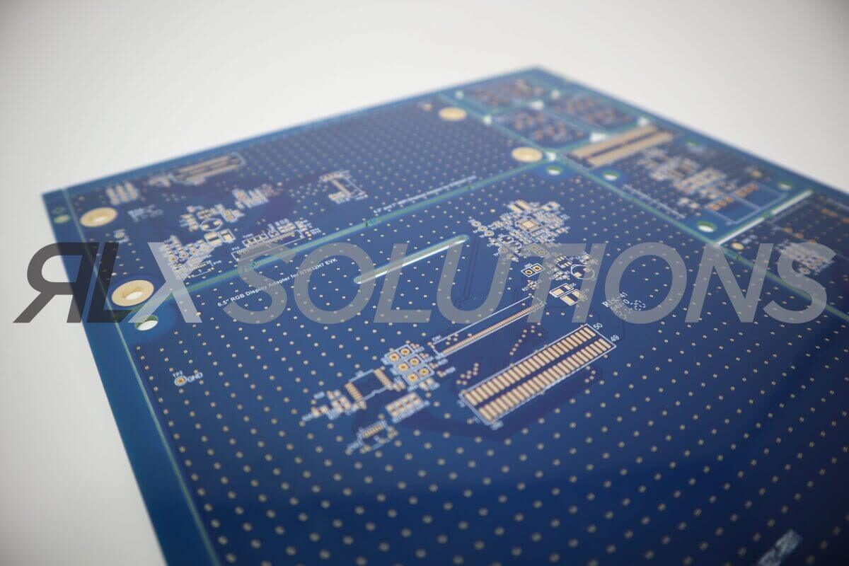
Fine-pitch SMT · 0.3 mm BGA capable · HDI microvias down to 0.10 mm laser drill
Request any service standalone or bundle them into a turnkey program. We coordinate the handoffs so you manage one quote and one program manager.
Bare PCB fabrication — FR-4, high-Tg, halogen-free, aluminum MCPCB, rigid-flex, polyimide, HDI, high-frequency. 1–24 layers standard.
View capabilities →Turnkey SMT, through-hole, and mixed-tech assembly. 01005 passives, 0.3 mm BGA pitch, conformal coat, functional test.
View capabilities →Obsolete, allocated, and hard-to-find parts. Authorized distribution plus verified excess-inventory sources. Full lot traceability.
View capabilities →Custom capacitors, industrial relay sockets, electronic packaging, terminal blocks, electro-mechanical interconnects.
View capabilities →Schematic capture, multi-layer layout, high-speed digital, thermal and power management. DFM / DFA review included.
View capabilities →Wire harnesses and custom cable assemblies for industrial, military, and medical applications. Crimping, over-molding, potting.
View capabilities →Searchable live inventory of electronic components. List your excess stock, or find the parts you need now.
Browse inventory →
Send Gerbers, BOM, and pick-and-place files. An engineer on our team reviews and responds with a real quote, DFM feedback, and timeline.
Boards, builds, and behind-the-scenes work from the RLX floor. Follow @rlxsolutions.