Rigid FR-4, high-Tg, halogen-free, aluminum MCPCB, rigid-flex, polyimide, HDI, and high-frequency substrates. 1–24 layers standard, up to 40 on request. Blind and buried vias, via-in-pad (POFV), controlled impedance ±10%. UL listed, ISO 9001:2015 certified, IPC-6012 Class 2 and Class 3 capable.
PCB manufacturing is the fabrication of the bare printed circuit board before any parts are placed. RLX Solutions manufactures rigid, multilayer, flex, rigid-flex, and metal-core boards in Canada for engineers and procurement teams who need verified specifications, traceable quality, and a quote within 24 hours.
We build the substrate, stackup, and process to the needs of your application. FR-4 standard and high-Tg for general-purpose builds. Aluminum MCPCB and copper-core for thermal-critical LED and power designs. Polyimide flex and FR-4/flex hybrid rigid-flex for compact and dynamic-bending applications. Rogers and PTFE for RF and high-frequency. HDI with stacked and staggered microvias for high-density designs.
Every PCB gets engineer-reviewed DFM before fabrication starts — no separate charge, no offshore handoff delay. Impedance-controlled stackups are verified by TDR on coupon with the test report shipped alongside the order. Class 3 builds follow the tighter annular-ring, copper-to-edge, and cross-section requirements — visible in the first-article documentation.
For the complete spec envelope (trace/space by layer count, minimum drills, surface finishes, via types, impedance ranges, and quality standards), see the Capability Reference on the home page.
Same quality system from the first five PCBs through the fifty thousandth. No setup re-do between tiers.
First-article builds with full DFM review. Quote response inside 24 hours. Ideal for design verification, debug, and pre-production validation.
Pre-production runs where DFM is locked and early-market delivery matters. First-article approval before the production lot.
Sustained production volume with scheduled delivery, AQL sampling, and full lot traceability per ISO 9001:2015 audit trail.
Tighter annular rings, plating specs, and cross-section sampling for medical, aerospace, and life-safety programs that require Class 3 workmanship.
Gerbers preferred for manufacturing. If you're earlier in the design cycle, send your native PCB design file and we'll extract what we need. Every submission receives engineering DFM review before quotation.
The standard envelope of every service we offer, organized the way an engineer evaluates a manufacturer: PCB parameters, drilling, traces, via types, surface finishes, impedance, special processes, and test. Specs are our routine production envelope. Anything beyond — 28-layer stackups, sub-2 mil traces, copper in >6 oz, controlled impedance tighter than ±5% — is available on request. Ask.
Pick the process you need from the tabs. Check your design against the specs. If your file passes, it's a routine build. If it doesn't, tell us what's off — 90% of edge cases are builds we quote without issue.
Recent production work — customer-specific details anonymized. Each of these passed full electrical test, AOI, and cross-section verification before shipment.
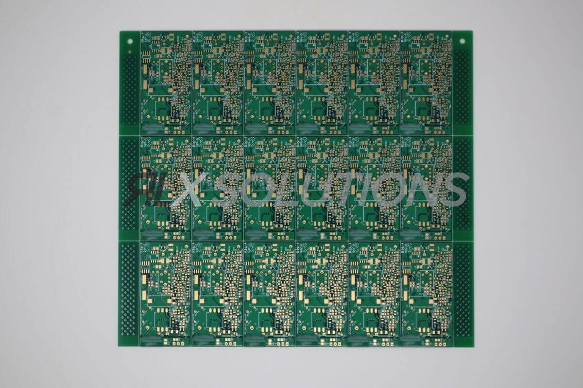
High-Tg FR-4, ENIG finish, panelized for volume SMT with fiducials and test coupons.
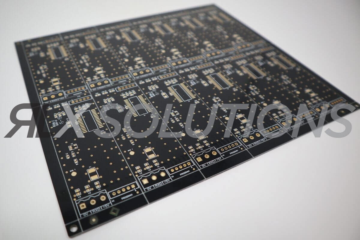
Matte black soldermask, white legend, ENIG gold-plated pads for fine-pitch BGA assembly.
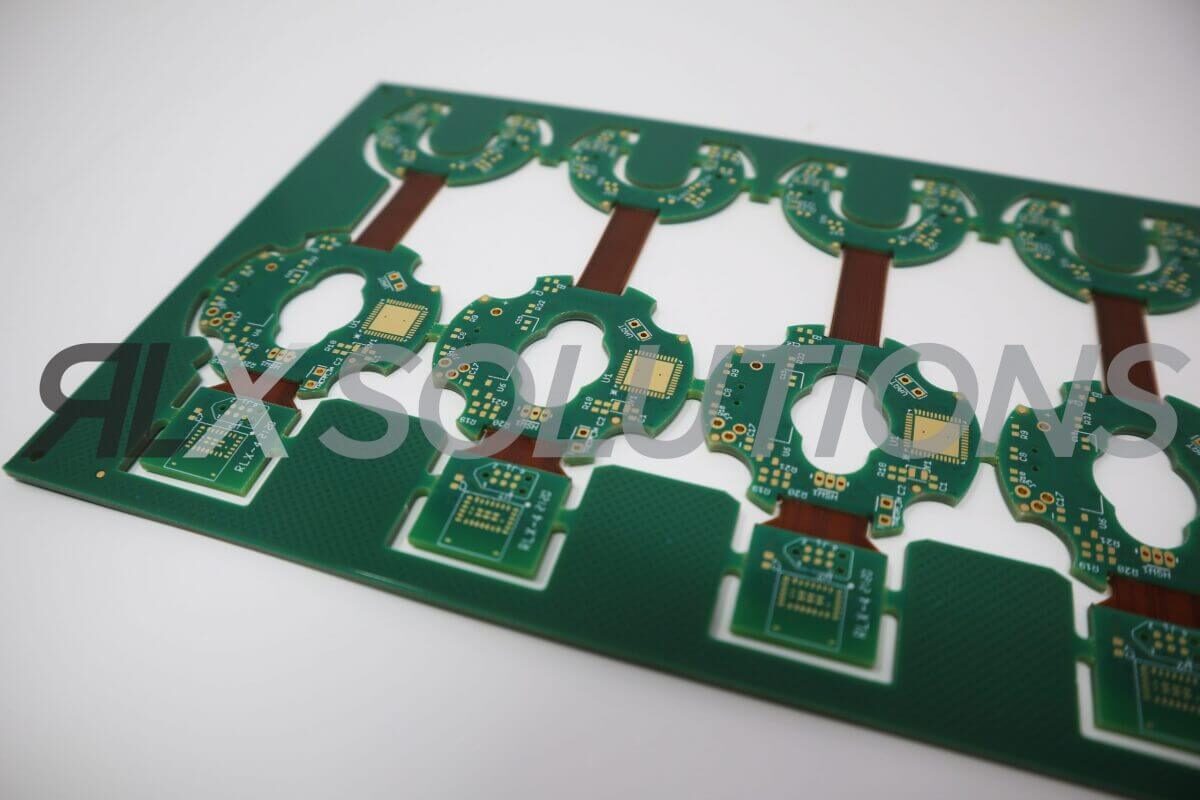
Polyimide flex ribbons connecting rigid FR-4 islands · bookbinder stackup for 3D assembly.
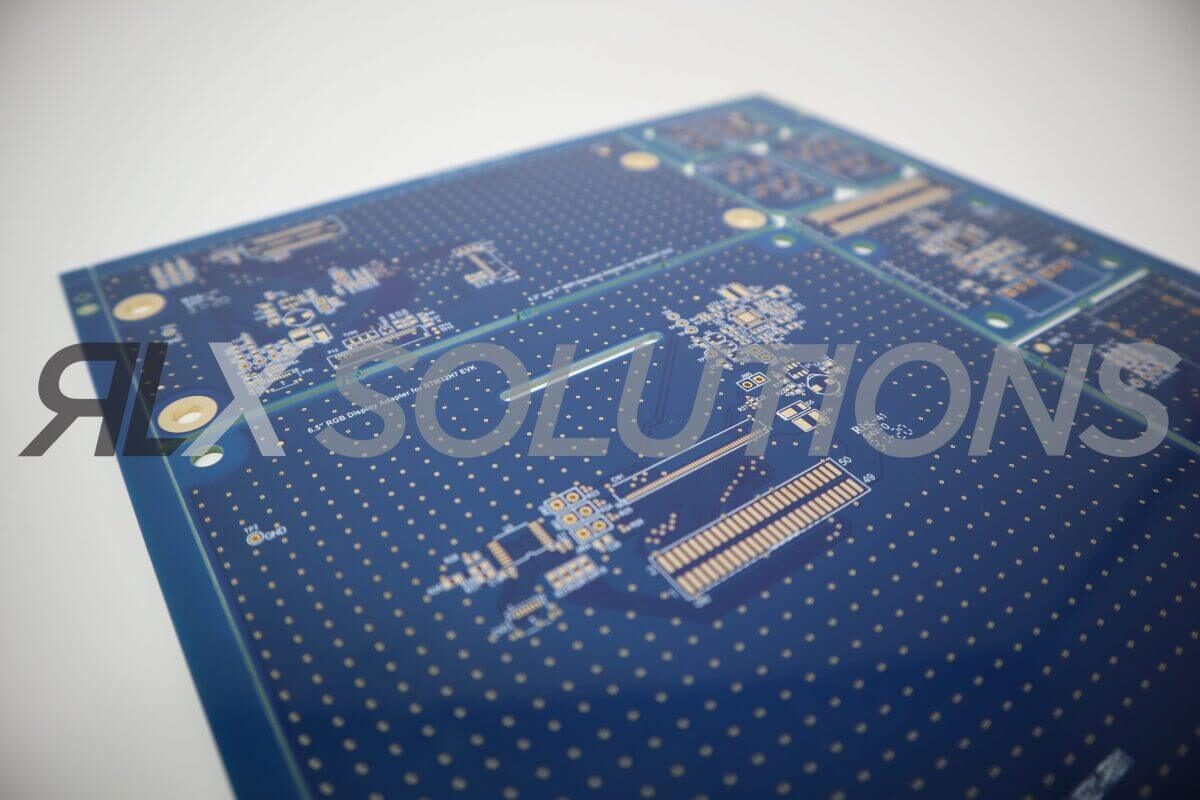
Blue soldermask, fine-pitch connectors, HDI microvia construction for high signal density.
Gerbers, stackup notes, impedance targets, and any fab callouts. An engineer reads every inquiry and replies with pricing, lead time, and DFM feedback.