
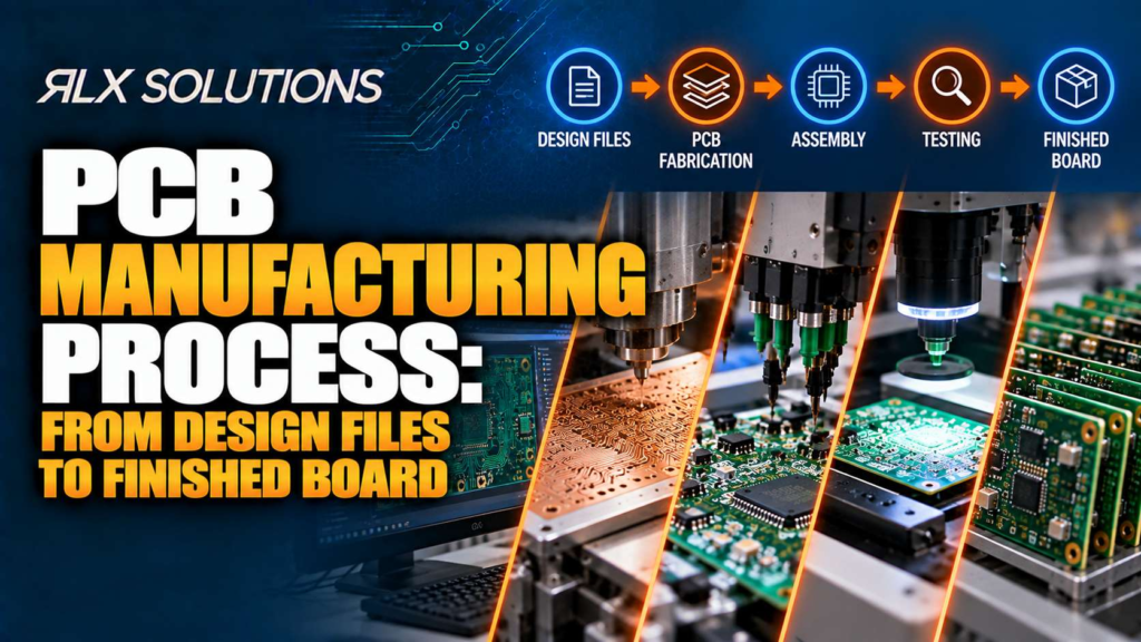
PCB Manufacturing Process From Design Files to Finished Board
The PCB manufacturing process converts released design data into a physical circuit board through engineering review, imaging, lamination, drilling, plating,
The PCB manufacturing process converts released design data into a physical circuit board through engineering review, imaging, lamination, drilling, plating,
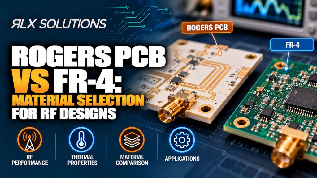
Rogers PCB materials generally make sense when RF performance depends on low dielectric loss, predictable impedance, or stable electrical behaviour
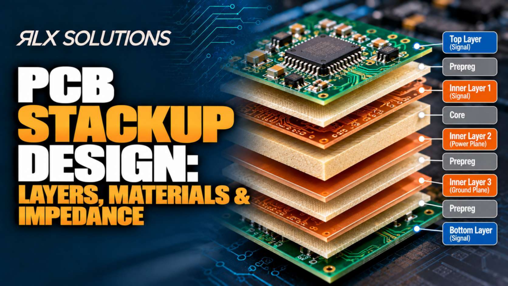
PCB stackup design defines how copper layers, dielectric materials, thickness and impedance targets work as one manufacturable structure. RLX Solutions,
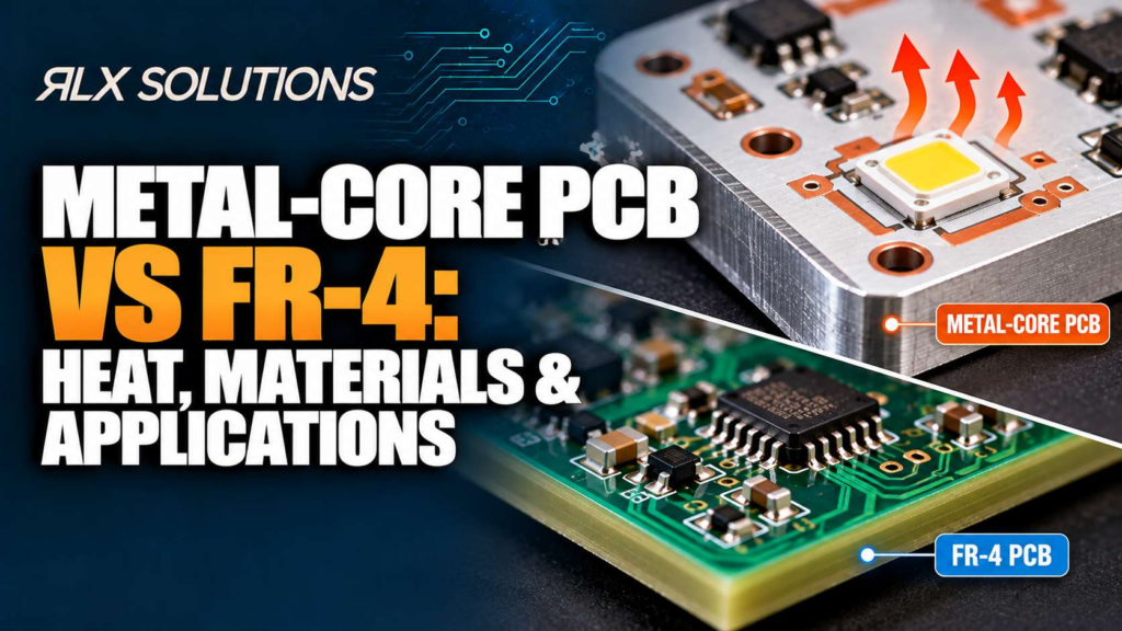
Metal-core PCB and FR-4 solve different board-level problems. Metal-core construction gives heat a short path into an aluminum or copper
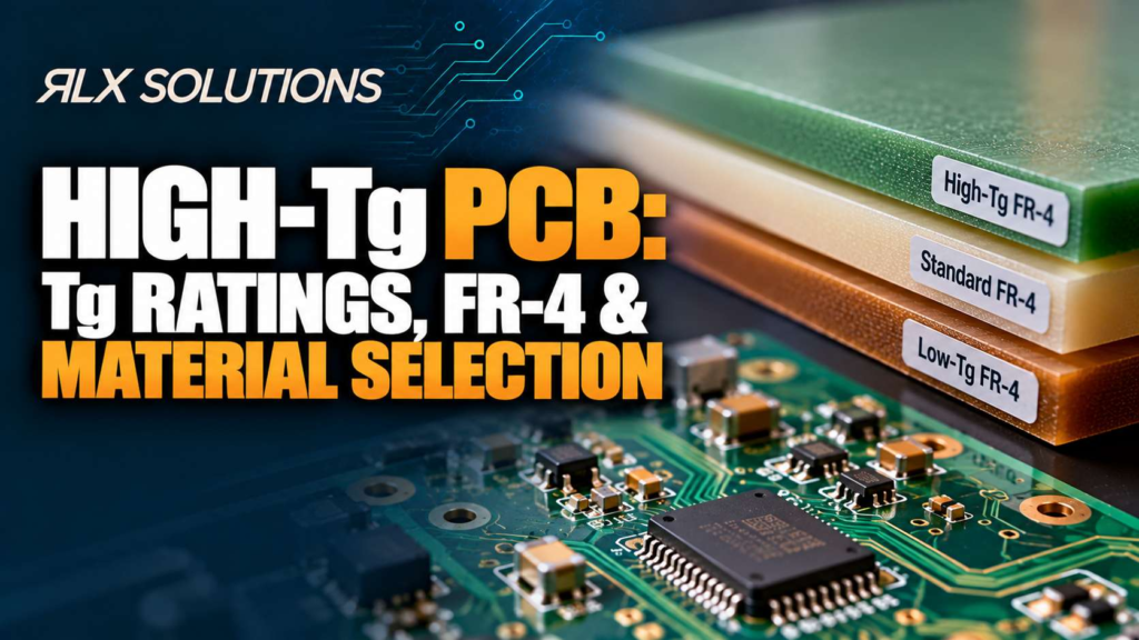
A high-Tg PCB uses laminate with a higher glass transition temperature so the board retains dimensional and mechanical stability through
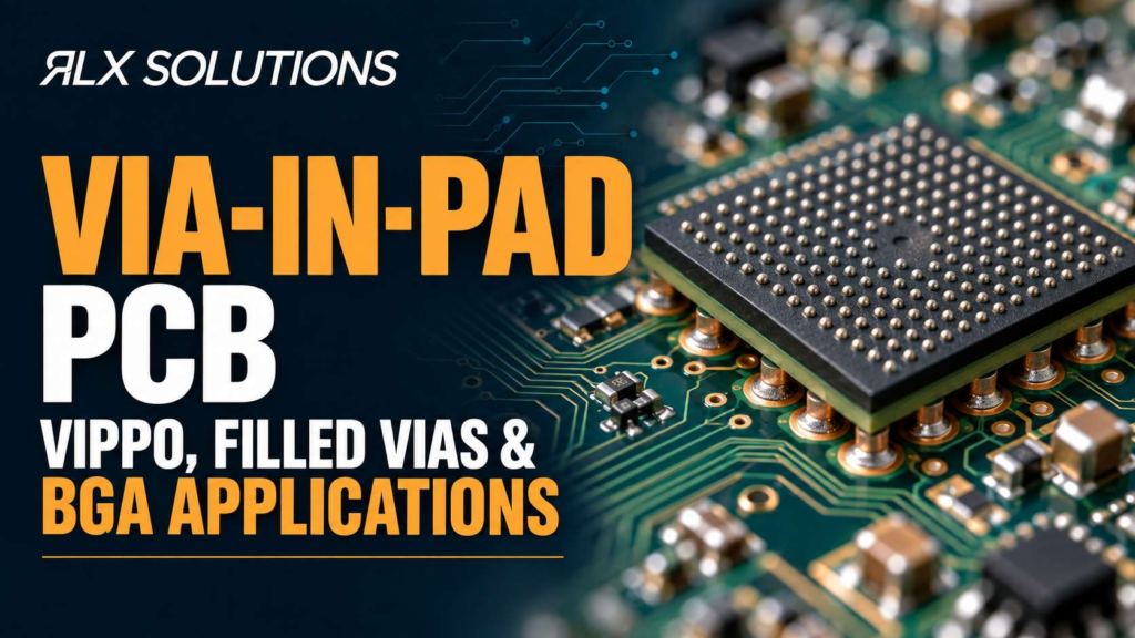
Via-in-pad places a via directly inside a component pad to shorten routing and create escape paths where conventional dog-bone fanout
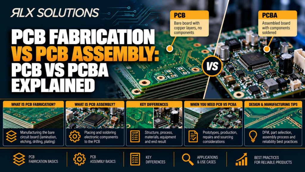
PCB fabrication produces the bare printed circuit board, while PCB assembly mounts and solders electronic components onto that board to
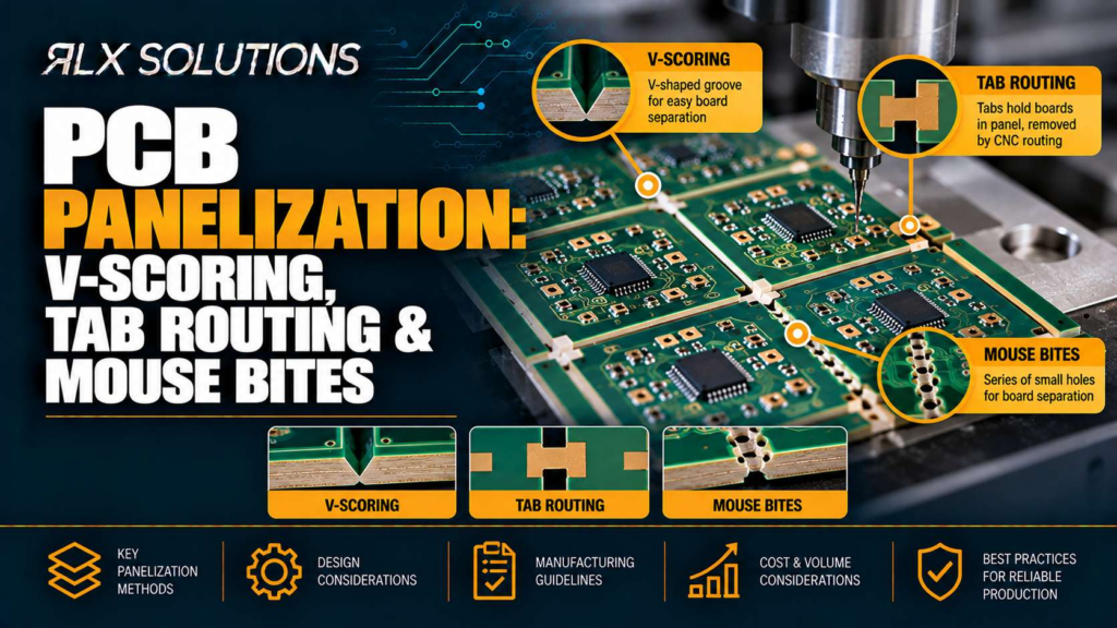
PCB panelization combines multiple circuit boards into a manufacturing panel, but the breakaway method affects board outline freedom, edge quality
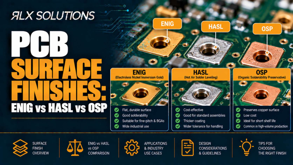
ENIG, HASL and OSP protect exposed PCB copper before assembly, but they create different pad surfaces and process constraints. ENIG
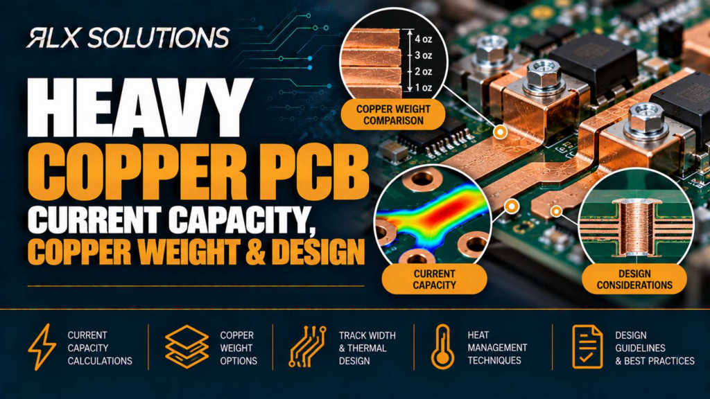
Heavy copper PCB current capacity depends on more than copper weight. Trace width, layer position, temperature rise, current path length,