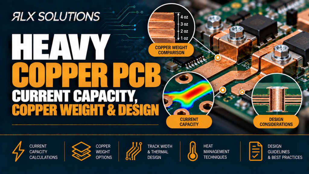
Heavy copper PCB current capacity depends on more than copper weight. Trace width, layer position,
temperature rise, current path length, vias and stackup all affect electrical and thermal performance.
RLX Solutions, a contract electronics manufacturer in Concord, Ontario, reviews heavy copper designs
against the complete current path rather than treating copper thickness as a standalone specification.
A heavy copper circuit board uses thicker conductors to increase copper cross-sectional area where the
design must carry substantial current, reduce resistive loss or spread heat. The design problem is not
simply how many ounces of copper you need. It is what conductor geometry keeps resistance, voltage drop
and temperature within the limits of the assembly.
That distinction matters because 4 oz copper can still produce a poor power path if the trace necks down
at a connector, crosses layers through an undersized via field or concentrates current around a thermal
relief. For the full picture, see our PCB Manufacturing Guide.
Current capacity starts with copper cross-section, not copper weight alone
Current flowing through a PCB conductor produces heat because the conductor has resistance. The basic
relationship is:
P = I2R
Doubling current increases resistive heating by a factor of four when resistance is unchanged. Increasing
copper cross-sectional area reduces resistance, but conductor temperature still depends on how effectively
the printed circuit board moves heat away from that copper.
For a rectangular PCB trace, cross-sectional area is determined mainly by trace width multiplied by
finished copper thickness. Copper weight is therefore one fabrication variable in a larger thermal and
electrical calculation.
| Design variable | Electrical or thermal effect |
|---|---|
| Higher copper weight | Increases conductor cross-section at the same trace width |
| Wider trace or plane | Reduces resistance and increases area available for heat spreading |
| Longer current path | Increases resistance and voltage drop |
| Higher current | Raises I2R heating rapidly |
| Higher ambient temperature | Reduces thermal margin |
| Layer transitions | Add via barrels and local current-density transitions |
| Trace neck-down | Creates local resistance and heating that can dominate the path |
Current capacity should therefore be treated as a thermal design problem rather than a fixed ampere
rating assigned to a copper weight. A 20 mm-wide plane and a 1 mm-wide trace can both use 4 oz copper
while having very different resistance and temperature behaviour.
Copper weight changes more than ampacity
Heavy copper changes the fabrication geometry of the entire circuit board. Outer copper can be specified
at 0.5, 1, 2 or 3 oz, with 4 to 6 oz outer copper available for designs that are reviewed against the
proposed stackup and geometry. Inner layers can use 0.5, 1 or 2 oz copper, with up to 3 oz inner copper
requiring similar stackup review.
As copper becomes thicker, etching is no longer well represented by the two-dimensional line width shown
in the CAD system. Copper must be removed through a deeper metal thickness, so trace width and spacing
become increasingly sensitive to etch geometry.
This is why a routing rule copied from a 1 oz board should not automatically be used on a 2 oz, 4 oz or
6 oz design. For example, a 2-layer board with 1 oz copper can use 3 mil trace and 3 mil space within the
fabrication envelope. At 2 oz, the corresponding geometry is 6 mil trace and 6 mil space.
Thicker copper may help electrically because a given trace gains cross-sectional area, but manufacturing
geometry can simultaneously require more spacing around that trace. Power routing and signal-density
planning therefore need to be solved together.
Design the complete high-current path
A high-current route is only as effective as its most restrictive section. If a large copper pour leaves
a connector, narrows between two pads, crosses layers through vias and then expands into an internal
plane, the wide regions do not eliminate the resistance of the narrow transition.
Three locations deserve particular attention: the pad-to-plane transition, any trace neck-down between
component pads, and the via field connecting layers. Each can run hotter than the surrounding copper
even when most of the net is a large polygon.
Worked example: a 4-layer power board
Consider a hypothetical 4-layer, 1.6 mm printed circuit board carrying a 12 A supply from an input
connector to a switching stage.
- Layer 1 uses 4 oz power copper.
- Layer 2 is ground.
- Layer 3 carries power distribution.
- Layer 4 carries control and secondary power.
- The main Layer 1 power path is 8 mm wide.
- A restriction beside a component footprint is 1.2 mm wide.
- The total high-current route is 70 mm long.
The 8 mm-wide section may have ample conductor area, but the 1.2 mm neck-down must be analysed separately.
Increasing the rest of the pour from 8 mm to 12 mm does little to reduce the local current density if all
12 A must still pass through the same 1.2 mm restriction.
That is why conductor geometry should be reviewed section by section instead of assigning one current
value to an entire net.
Temperature rise belongs in the design requirement
Trace sizing needs an allowable temperature rise, not just an expected current. Current raises the copper
temperature above the local ambient, and that additional heat affects the laminate, nearby components,
connectors and any enclosure-level thermal assumptions.
A high-current PCB specification should establish:
- Maximum continuous current
- Peak current and peak duration
- Ambient temperature range
- Acceptable conductor temperature rise
- Duty cycle
- Cooling assumptions
- Maximum acceptable voltage drop
Current waveform matters. A rail carrying 15 A continuously creates a different thermal condition from
a rail that reaches 15 A briefly during motor startup and then operates at a much lower steady current.
The copper geometry should reflect that operating profile.
Voltage drop can force larger copper before temperature does
A conductor can satisfy a temperature-rise objective and still create too much voltage loss. Conductor
resistance follows:
R = ρL/A
Resistance increases with conductor length and decreases as cross-sectional area increases. Voltage drop
then follows:
V = IR
and conductor power loss remains:
P = I2R
For low-voltage, high-current rails, voltage drop can become the tighter constraint. Two boards with the
same copper weight and trace width may therefore require different power geometries if one routes current
25 mm and the other routes it 180 mm.
The layout response might be a wider conductor, heavier copper, a shorter route, parallel copper on
multiple layers or different component placement. The electrical target should choose the geometry rather
than a preference for thicker foil by itself.
Board A vs Board B: same layer count, different manufacturing cost
Layer count alone does not describe heavy copper fabrication difficulty. Consider two hypothetical
6-layer boards with the same external dimensions.
| Decision factor | Board A | Board B |
|---|---|---|
| Layer count | 6 layers | 6 layers |
| Outer copper | 2 oz | 4 oz |
| Inner copper | 1 oz | 2 oz |
| Power routing | Wide Layer 1 pours | Dense Layer 1 power routing |
| Layer transitions | Through vias | Multiple high-current via fields |
| Fine routing near power section | Limited | Dense |
| Main manufacturing challenge | Board area | Heavy copper beside dense geometry |
Board A can achieve current capacity through wider copper because routing area is available. Board B uses
thicker copper because its power section must share space with dense control circuitry.
Board B introduces additional fabrication interaction even though both designs have six layers. Thicker
copper influences etching and spacing while the dense local routing reduces the geometric margin available
to absorb those changes.
A useful layout response is to separate the dense control section from the heavy-current area where
practical. That creates more room to maintain copper spacing, pad geometry and current-path width without
forcing every part of the PCB into the same routing rules.
Vias can become the bottleneck when current changes layers
A high-current path that changes layers must transfer that current through plated copper. The design
problem therefore expands from trace width into hole diameter, finished plating, via count, pad geometry
and how evenly current enters the via field.
A broad power plane connected through one or two vias may be electrically continuous in the CAD system,
but continuity is not the same as adequate current capacity.
Worked example: one 20 A transition, two layouts
Consider a hypothetical 8-layer PCB that must move a 20 A rail from a Layer 1 copper region to a Layer 3
power region.
Option A uses four vias placed in a tight row beside the connector pad.
Option B distributes twelve vias across the width of the copper transition.
Both arrangements connect Layer 1 and Layer 3. Option B creates more parallel conductive paths and spreads
current across a broader transition. It also reduces the chance that the entire current path funnels
through a small copper neck before reaching the via array.
The final via count still cannot be chosen from current alone. Hole geometry, plating, pad dimensions,
board thickness and the available copper around the array must be evaluated together.
Mechanically drilled plated through-holes can use a minimum 0.15 mm drill, while board thickness and hole
diameter are also constrained by aspect ratio. A 10:1 maximum aspect ratio is standard, with 12:1 builds
requiring review against the actual stackup. On a thick power board, this relationship can affect the via
strategy before routing is complete.
Heavy copper affects pads, clearances and component escape routing
Heavy copper design often becomes difficult where power geometry meets dense component geometry. A
switching device can require a broad drain or source connection while its gate circuitry needs narrow
signal routing nearby. A power connector can carry substantial current while adjacent pins are used for
sensing or control.
Review these locations before layout release:
- Trace neck-down between pads
- Copper spacing beside thick power features
- Solder-mask dams near power footprints
- Copper-to-board-edge clearance
- Thermal-relief spokes on high-current pads
- Via fields that consume escape-routing space
- Large copper imbalance between different board regions
Copper-to-edge clearance is another physical constraint. A minimum 0.3 mm copper-to-edge clearance means
a power polygon cannot simply be expanded until it reaches the routed board profile.
Pad and solder-mask geometry also need to be reviewed together. Thick copper does not remove the need for
manufacturable mask dams and pad clearances in the same region.
Do not add heavy copper to every layer by default
More copper is not automatically a better stackup. If only the input and output stages carry substantial
current, increasing copper thickness across every layer can introduce manufacturing constraints without
solving a useful electrical problem.
Map the current paths before assigning copper weight:
- Identify each source and load.
- Mark continuous and transient current.
- Locate unavoidable neck-downs.
- Identify every layer transition.
- Calculate voltage-drop-sensitive sections.
- Mark copper that is required mainly for heat spreading.
- Separate heavy-current routing from dense signal routing where practical.
Then assign copper weight by layer based on what each layer must do. Outer and inner layers do not need
identical copper weights. A multilayer board may benefit from heavier outer copper for accessible power
routing while keeping internal signal layers lighter for routing density.
That decision should happen during stackup development rather than after detailed routing is finished.
Surface finish and assembly still matter on a power board
Copper thickness solves only the conductor portion of the problem. Components still have to solder
reliably to the bare PCB, and large copper features can change how heat moves through a component pad
during assembly.
Available surface finishes include tin-lead hot air solder levelling, lead-free SnCuNi hot air solder
levelling, electroless nickel immersion gold, electroless nickel electroless palladium immersion gold,
immersion silver, immersion tin, organic solderability preservative and hard gold for appropriate contact
features.
Finish selection should follow component, assembly and product requirements rather than copper weight
alone.
Large power planes also affect soldering because they can pull heat away from a pad. Thermal-relief
geometry, component thermal mass and the soldering process need to be considered together. Where hidden
solder joints are present, inspection may also involve X-ray in addition to solder paste inspection,
automated optical inspection and manual inspection.
Heavy copper is therefore a bare-board decision with direct assembly consequences.
Put these requirements in the fabrication package
A manufacturer can review a high-current circuit board more effectively when the electrical intent is
supplied with the manufacturing geometry. Fabrication data can be provided as Gerber RS-274X, ODB++ or
IPC-2581 along with NC drill data, stackup information, impedance requirements where applicable and
fabrication notes.
For the heavy copper portion of the design, identify:
- Copper weight by layer
- Finished board thickness
- High-current nets
- Continuous and peak current conditions
- Temperature-rise assumptions
- Voltage-drop requirements
- Critical via transitions
- Any required filled or capped via structures
- Stackup constraints that cannot change
Do not rely on the visual size of a polygon in the PCB editor to communicate electrical priority. A large
copper region might function as a current path, heat spreader, shield or several of those at once.
Fabrication notes should make the requirement clear enough for engineer-reviewed design for
manufacturability, or DFM, to catch conflicts before production.
Treat heavy copper as a stackup decision
The best point to choose heavy copper is before final routing. Changing a completed design from 1 oz to
4 oz copper may require more than editing a fabrication note. Spacing, pad clearances, neck-downs,
impedance structures and component escape routes may all need to be reconsidered.
A stronger design sequence is:
Electrical load → thermal target → conductor geometry → copper weight → stackup
→ detailed routing
This sequence also exposes cases where heavy copper is unnecessary. If placement changes can shorten the
current path or create room for a much wider conductor, the design may meet its resistance and thermal
targets without pushing the entire board toward thicker copper.
If the design genuinely requires 4 to 6 oz outer copper, that decision should be made early enough for
spacing, drilling, pad geometry and assembly requirements to develop around the chosen stackup.
Get the power geometry reviewed before release
If your PCB uses heavy copper, high-current layer transitions or a stackup combining dense signals with
4 to 6 oz outer copper, RLX can review the manufacturing data as part of the quote process. Send the
fabrication files, stackup and relevant design documentation so the electrical intent can be checked
against the proposed build before production.
Frequently Asked Questions
How much current can a heavy copper PCB carry?
There is no single ampere rating for heavy copper. Current capacity depends on copper thickness, trace
width, path length, layer position, allowable temperature rise and the surrounding thermal environment.
A wide 4 oz plane and a narrow 4 oz trace have different resistance and thermal behaviour even though
their copper weight is identical.
Is 3 oz copper considered heavy copper?
Terminology varies between designers and manufacturers, so the better purchasing specification is the
actual copper weight required by layer rather than relying on the label heavy copper. The manufacturing
issue is that increasing copper thickness changes etching, trace spacing and the interaction between
power features and nearby dense routing.
Can I use 6 oz copper on a PCB?
Yes. Up to 6 oz outer copper can be considered for an appropriate board design, but the actual stackup
and feature geometry need review. Thick copper affects etching, spacing, pads and routing density, so
establish the copper requirement before completing detailed layout rather than changing foil weight
after routing.
Should high-current traces be on outer or inner layers?
Choose the layer from the complete electrical, thermal and routing problem rather than current alone.
Outer-layer copper can provide direct component access and useful heat-spreading area, while internal
planes can distribute power through a multilayer design. Copper-weight availability also differs between
outer and inner layers, making stackup planning part of the decision.
Do I need multiple vias for a high-current PCB trace?
A layer transition should be treated as its own conductor structure. Multiple vias can provide parallel
current paths, but the arrangement depends on hole geometry, plating, pad dimensions, board thickness
and current distribution into the via field. Also check for copper neck-down around the array because
additional vias cannot correct a restricted approach path.
What files should I send for a heavy copper PCB quote?
Provide complete bare-board manufacturing data such as Gerber RS-274X, ODB++ or IPC-2581 files, NC
drill data, stackup information and fabrication notes. Clearly identify copper weight by layer and any
electrically critical requirements. Assembly projects additionally require the bill of materials,
pick-and-place or centroid data and assembly drawing.