
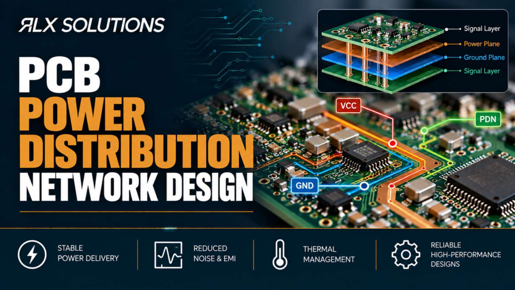
PCB Power Distribution Network Design
PCB power distribution network design is the process of controlling impedance from the power source to each load across the
PCB power distribution network design is the process of controlling impedance from the power source to each load across the
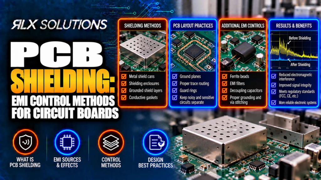
PCB shielding works best when it is treated as part of the electromagnetic interference (EMI) control strategy, not as a
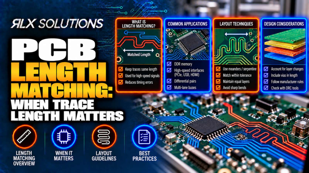
PCB length matching controls the relative arrival time of signals that must remain synchronized. The design target is therefore timing,
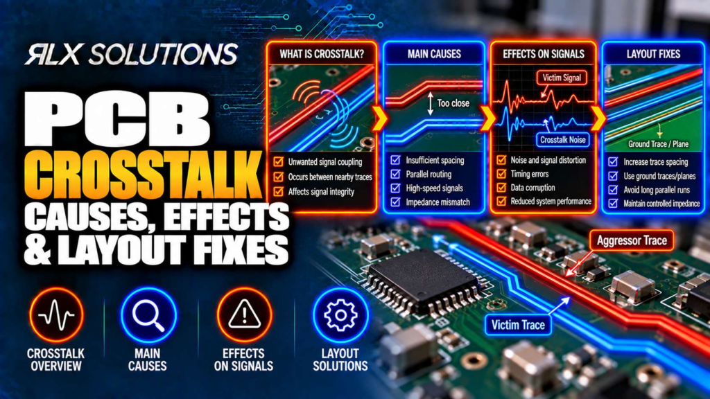
PCB crosstalk is unwanted electromagnetic coupling from one signal path into another, driven mainly by trace geometry, edge rate, reference-plane
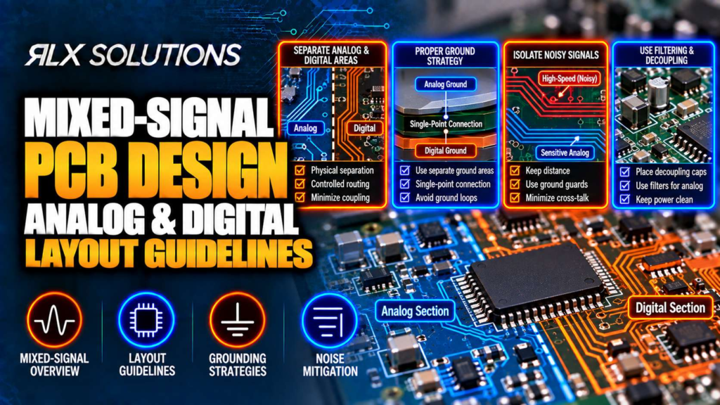
Mixed-signal PCB design works when analog and digital currents are controlled by placement, return-path geometry, power distribution and routing rather
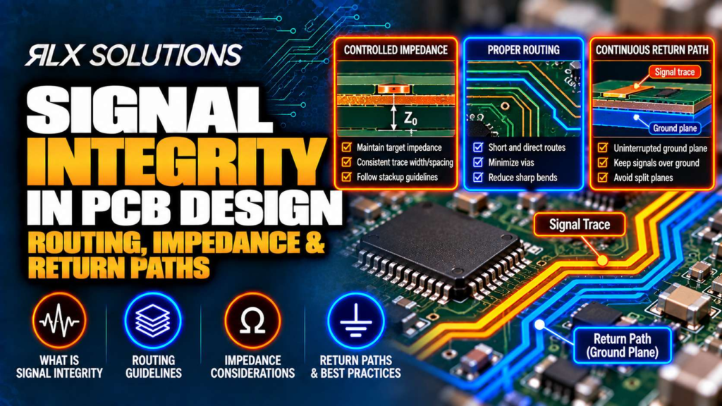
Signal integrity in PCB design depends on treating the trace and its return path as one electromagnetic structure. Controlled impedance,
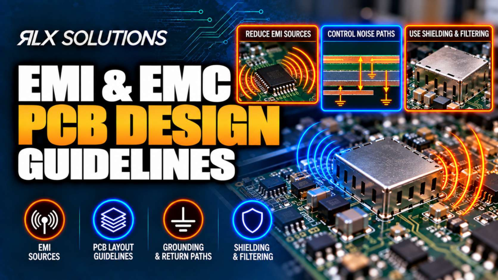
Electromagnetic interference (EMI) is controlled most effectively in the PCB layout, not after a compliance failure. Good electromagnetic compatibility (EMC)
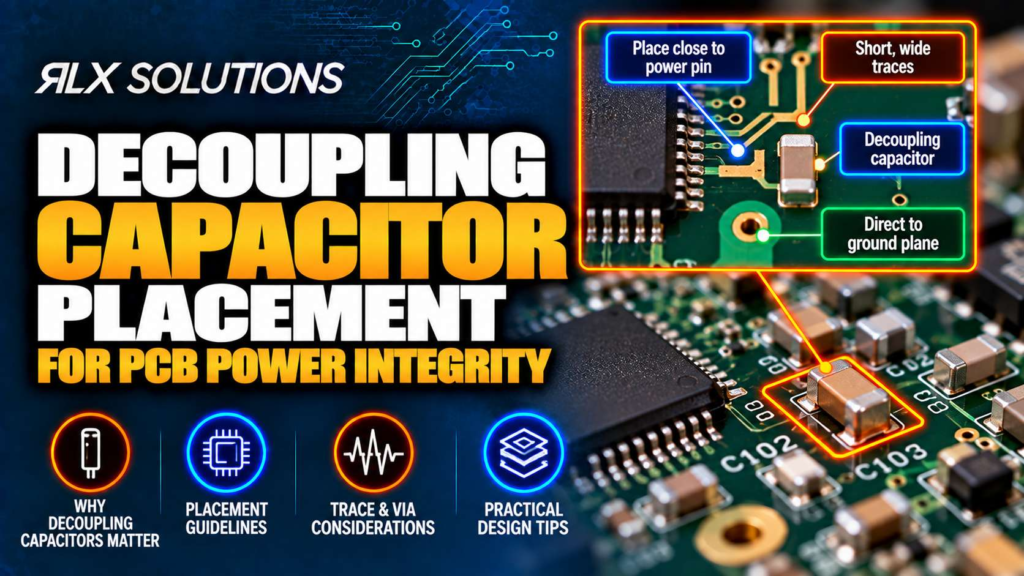
Decoupling capacitor placement is a power integrity problem, not a distance-to-pin rule. The capacitor must provide a low-impedance current path

PCB thermal management starts by giving heat a low-resistance path away from power components and hot spots. Copper area, copper
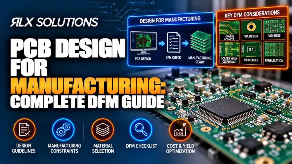
PCB design for manufacturing (DFM) means designing the printed circuit board around the fabrication, assembly and test processes that will