

Multilayer PCB Manufacturing: Layer Count, Stackups, Cost & Lead Time
Multilayer PCB manufacturing gets more expensive and schedule-sensitive as the stackup adds material, registration demands, drilling steps and lamination cycles.
Multilayer PCB manufacturing gets more expensive and schedule-sensitive as the stackup adds material, registration demands, drilling steps and lamination cycles.
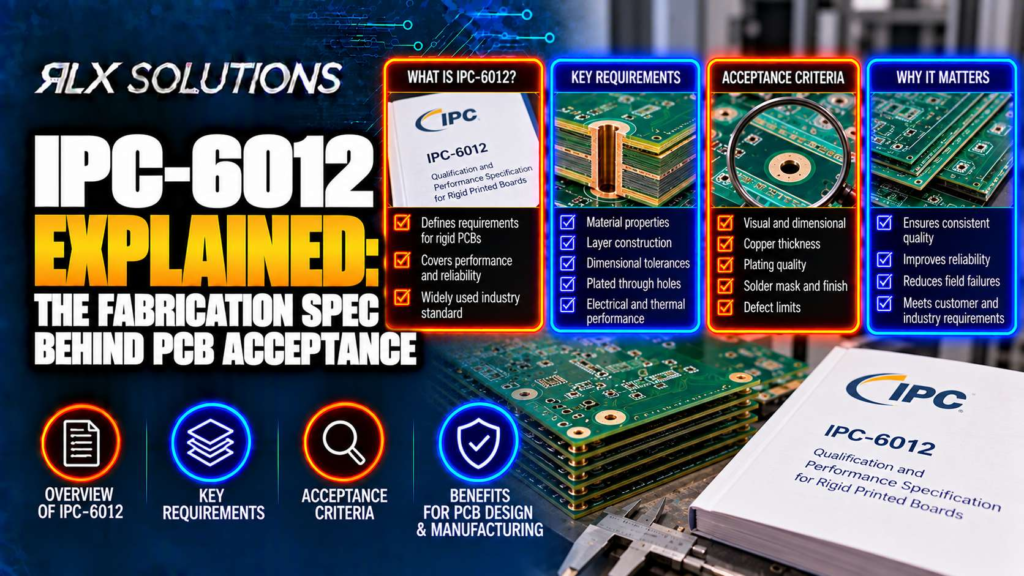
IPC-6012 defines qualification and performance requirements for rigid printed circuit boards, turning design intent into fabrication acceptance criteria. RLX Solutions,
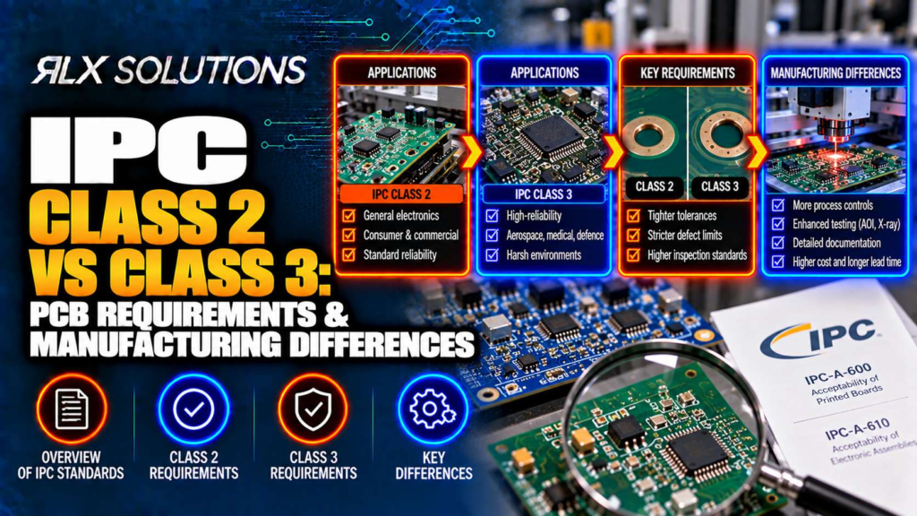
IPC Class 2 vs Class 3 is primarily a difference in the required level of manufacturing assurance, workmanship and acceptance

Choosing a PCB manufacturer starts with matching your actual board construction to a documented manufacturing process, then verifying how quality
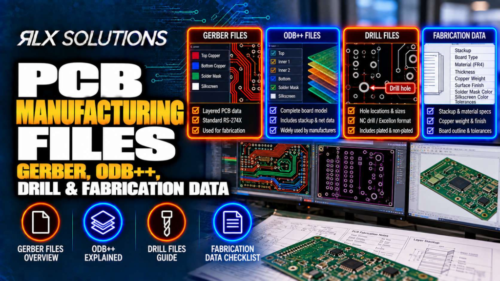
PCB manufacturing files tell a fabricator what copper to image, where to drill, how to build the stackup and which
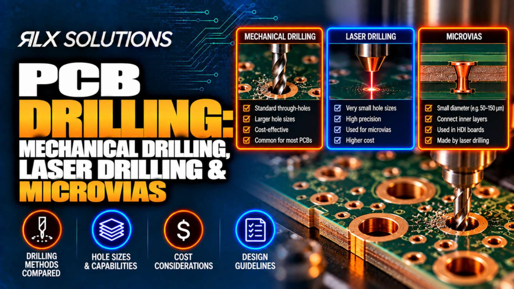
PCB drilling method follows the interconnect geometry, not simply the layer count. Mechanical drilling suits plated through-holes and larger features,
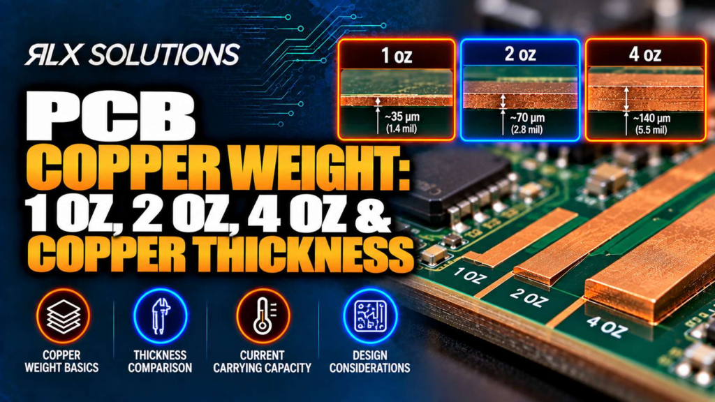
PCB copper weight describes the nominal copper thickness produced when a specified mass of copper is spread over one square
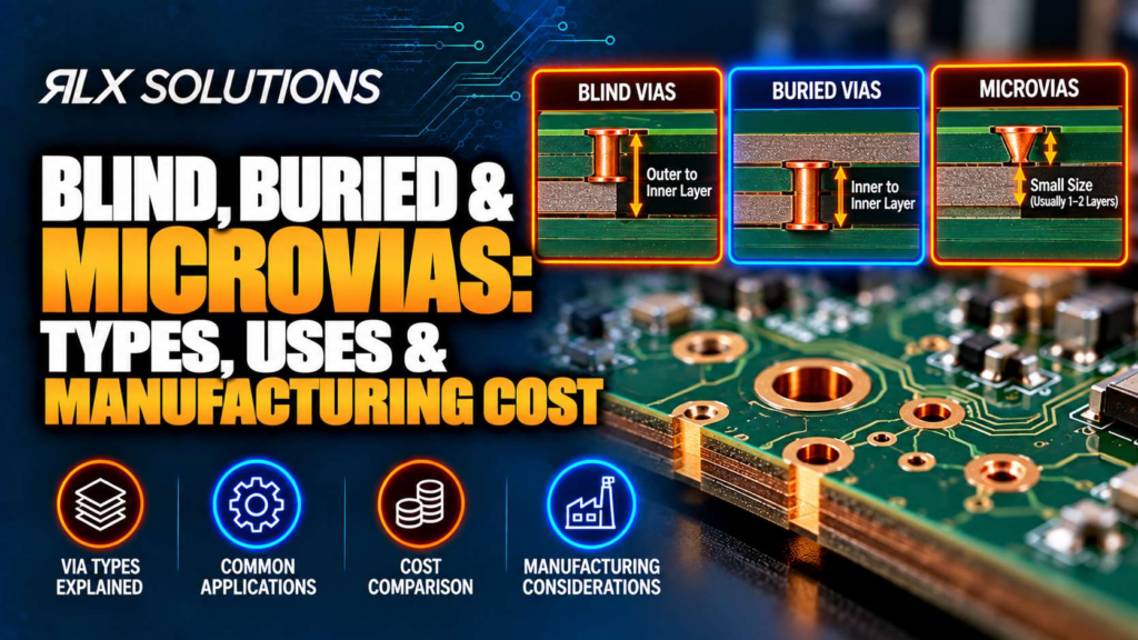
Blind vias connect an outer layer to one or more inner layers, buried vias connect only internal layers, and microvias
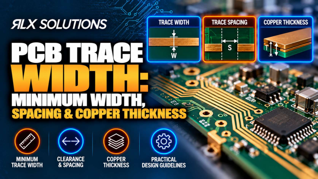
PCB trace width and spacing cannot be specified independently of copper thickness. A geometry that is practical in 1 oz
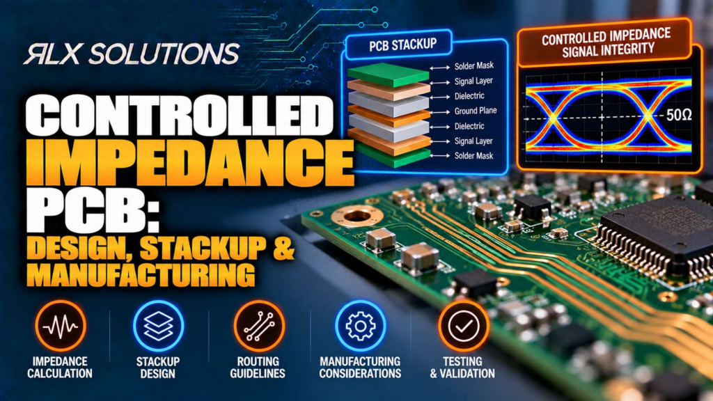
A controlled impedance PCB holds transmission-line impedance within a specified tolerance by controlling trace geometry, dielectric construction and copper characteristics