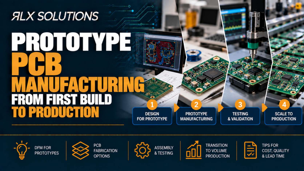
Prototype PCB manufacturing turns a design into hardware that can expose electrical,
mechanical and manufacturing problems before they multiply at volume. RLX Solutions,
a contract electronics manufacturer in Concord, Ontario, treats the first build as the
beginning of a controlled path toward repeatable production, not as an isolated batch
of working boards.
The difference matters. A prototype can power up correctly and still carry problems
that become expensive at 500 or 5,000 pieces: marginal drill geometry, difficult
assembly access, a component with weak supply continuity, an unproven test method,
or fabrication notes that leave too much open to interpretation.
A useful prototype therefore answers two questions at once: does the circuit work,
and can the same design be built repeatedly?
Prototype manufacturing should test the process as well as the circuit
A prototype is a low-volume build used to validate a design before production
quantities are committed. A bare PCB is the fabricated circuit board before
components are installed. Once components are placed and soldered, the result is a
printed circuit board assembly, commonly shortened to PCBA.
Those distinctions matter because fabrication, assembly and functional validation
can expose different failures.
A fabrication problem may appear as an impedance deviation, an unsuitable via
structure or a stackup that cannot be produced as drawn. An assembly problem may
come from paste deposition, package geometry or polarity documentation. A functional
problem may not appear until firmware is loaded and the board operates under realistic
electrical conditions.
Treating prototype PCB manufacturing as a miniature production exercise gives the
engineering team more useful evidence than asking only whether five boards turn on.
That does not mean freezing every production detail before the first build. Early
prototypes still exist to support change. It means recording the assumptions that
matter later: stackup, laminate, copper, drill structure, finish, bill of materials,
assembly revision, programming method and test criteria.
The first build should produce information, not just hardware
Suppose an eight-layer control board reaches the bench and all five prototypes pass
functional test. That result confirms something important, but it does not answer
every production question.
If two connectors were manually adjusted during assembly, a substitute regulator
was purchased for the prototype lot, and test technicians probed convenient component
leads because formal test points do not exist, those five passing boards have
identified three production tasks rather than completed the validation cycle.
The design may be electrically sound while the manufacturing process is still unfinished.
Start with fabrication choices that can survive the next quantity break
PCB fabrication converts the released manufacturing data into the physical board
through imaging, lamination, drilling, plating, solder mask, surface finishing and
electrical verification. Choices made before the first prototype affect how many
of those operations the board requires.
Layer count alone is therefore a weak predictor of manufacturing difficulty.
Consider two hypothetical 10-layer boards:
| Decision factor | Board A | Board B |
|---|---|---|
| Layer count | 10 layers | 10 layers |
| Via structure | Through vias only | Layer 1 to 2 microvias, Layer 2 to 3 microvias, buried vias between inner layers |
| Lamination | Conventional multilayer build sequence | Sequential lamination required by blind and microvia structures |
| Via-in-pad | None | Filled and capped pads under selected components |
| Manufacturing effect | Fewer dependent operations | More drilling, filling, plating and lamination dependencies |
| Main engineering question | Can through vias meet routing density? | Is the added density worth the added process sequence? |
The two boards have the same layer count, but Board B can cost more because its
interconnect architecture creates more manufacturing stages. A blind via terminates
on an internal layer rather than passing through the entire board, so the relevant
layers must be built and processed in a sequence that allows the hole to be formed
and plated before the remaining stack is completed.
A microvia is a laser-drilled small-diameter interconnect used for dense layer-to-layer
routing. When it lands in a component pad, resin fill, copper capping and planarization
can become part of the manufacturing sequence so the assembly surface remains suitable
for soldering.
That is why an engineer should ask how the via structure changes the process, not
simply how many layers are in the stack.
Hole diameter and board thickness belong in the same decision
Aspect ratio is the relationship between hole depth and drilled diameter. As a plated
hole becomes deeper relative to its diameter, achieving consistent copper deposition
through the barrel becomes more demanding.
Take a hypothetical 1.6 mm thick board.
A 0.20 mm through hole produces an 8:1 thickness-to-hole relationship. Reducing the
hole to 0.15 mm on the same 1.6 mm board pushes that relationship to roughly 10.7:1.
That change may look small in the CAD tool, but it changes the fabrication problem.
One option is to reconsider the finished board thickness or hole diameter. Another is
to change the interconnect architecture rather than forcing one small mechanical drill
through the full stack.
Within RLX fabrication, the standard maximum aspect ratio is 10:1, with 12:1 scoped
per project. The minimum mechanical plated through-hole drill is 0.15 mm, while
laser-drilled microvias can reach 0.10 mm. Those values should be evaluated together
rather than treated as unrelated entries on a fabrication drawing.
Use prototype DFM to remove avoidable production constraints
Design for manufacturability, or DFM, is the process of reviewing a design against
the way it will actually be fabricated and assembled. Good DFM does more than detect
a hard process violation. It identifies design choices that consume manufacturing
margin without delivering useful electrical or mechanical benefit.
That distinction becomes more important as quantity rises.
A prototype may justify a dense escape pattern because the layout is still being
validated. Once the design stabilizes, a second review can ask whether every narrow
trace, small drill or complex via remains necessary.
For example, imagine a six-layer board using 3 mil trace and 3 mil spacing in one
congested processor escape region while the remaining routing has significantly more
room. Preserving the fine geometry only where density requires it gives manufacturing
more latitude elsewhere than forcing the complete design toward the densest feature.
Copper weight changes the same calculation. On a two-layer board with 1 oz outer
copper, 3 mil trace and 3 mil spacing is within the stated fabrication envelope.
Moving the design to 2 oz copper changes the listed trace and spacing value to
6 mil / 6 mil. The added conductor thickness affects the etching problem, so a layout
that worked at one copper weight should not be assumed to transfer unchanged to another.
The production question is not whether a fabricator can make the hardest feature
once. It is whether that feature still deserves to exist across every board in the lot.
The prototype BOM is already a production document
The bill of materials, or BOM, defines what must be purchased and installed. During
prototyping it is tempting to treat sourcing as a temporary problem because the
immediate objective is to obtain enough parts for a handful of boards.
That can create a false sense of design maturity.
A footprint may be correct while its selected component is approaching end of life.
A processor may work perfectly while supply is allocated. An apparently interchangeable
substitute may differ in temperature range, package variant or another parameter that
matters to the finished product.
Production readiness therefore requires the engineering and procurement teams to
resolve both electrical suitability and sourcing identity.
Useful BOM data should remove ambiguity around manufacturer, manufacturer part number
and any permitted substitutions. Critical or long-lead components also need a sourcing
decision before a pilot lot creates pressure to accept a replacement simply because
it is available.
Counterfeit risk enters the same discussion when a required part moves outside normal
authorized supply. Authenticity controls can include source vetting, package and
date-code inspection, visual inspection, lot verification, X-ray and electrical
testing, with further analysis where the risk justifies it.
The principle is simple: a working prototype does not prove that its component supply
path can support production.
Assembly turns layout decisions into process behaviour
Surface mount technology (SMT), through-hole assembly and mixed-technology builds
translate PCB geometry into soldering and placement operations. Once the bare board
reaches assembly, features that looked acceptable on screen begin interacting with
stencil apertures, solder paste, component packages, reflow and inspection.
A dense package makes this visible.
Imagine a hypothetical board with a 0.5 mm pitch ball grid array beside several
0201 passives. The board may be electrically correct, but production planning still
has to address paste deposition, pad geometry, component orientation, inspection
access and any test strategy for joints that cannot be seen directly.
At finer geometry, inspection becomes part of the process design rather than a final
cosmetic check.
Solder paste inspection (SPI) measures deposited paste before reflow. Automated
optical inspection (AOI) examines assembled surfaces after reflow. Automated X-ray
inspection (AXI) can evaluate hidden joints beneath packages such as BGAs, land grid
arrays and quad-flat no-lead devices.
The relevant lesson from the prototype is not simply that the parts were placed
successfully. It is whether the manufacturing and inspection sequence can detect
the defects you care about before the build reaches volume.
Via-in-pad affects assembly as well as fabrication
A via placed directly in a surface-mount pad creates an interaction between fabrication
and soldering. If the via remains open, solder can migrate into the hole during
assembly and reduce the solder volume available at the joint.
Filled and capped via-in-pad addresses that mechanism by closing and planarizing the
feature before assembly.
This is why high-density interconnect choices cannot be reviewed only by the PCB
layout team. The fabrication method changes the solderable surface presented to assembly.
Build the test strategy before the pilot lot
Testing becomes harder to retrofit after routing, component placement and mechanical
constraints are fixed.
Flying-probe in-circuit testing can suit prototype and low-volume work because it can
access electrical nets without a dedicated bed-of-nails fixture. At production
quantities, fixture-based in-circuit testing may become appropriate where the product
and programme justify it. Functional test then evaluates the assembled board against
the customer’s required operating behaviour.
These methods answer different questions.
Electrical net testing can find opens and shorts. In-circuit testing can exercise
accessible nodes and component-level conditions. Functional testing verifies that
the finished assembly performs the required function under the defined test procedure.
A board that passes one category has not automatically passed the others.
Consider a hypothetical motor-control board with 140 accessible electrical nets.
During the first build, flying probe can cover those nets without committing to a
production fixture. If the design later enters a 2,000-piece production programme,
the team can decide whether fixture-based test offers enough repeatability and
throughput to justify locking test access into the design.
If that discussion starts only after the pilot build, mechanical placement may already
have consumed the accessible locations.
First article approval is the gate between intent and repetition
A first article is the initial build inspected against the released design and
manufacturing requirements before the larger production lot is released. Its purpose
is to prove that the documented process produced the intended assembly.
This is a different milestone from receiving an early engineering prototype.
A prototype can still carry temporary substitutions, hand modifications or open design
questions. A production first article should correspond to the revision that
procurement, manufacturing, inspection and test are expected to repeat.
That makes revision control central to the handoff.
If the schematic is Rev C, the Gerbers are Rev D, the BOM still contains a Rev B
component substitution and the assembly drawing was exported before a connector
orientation changed, the problem is no longer circuit design. It is configuration control.
Production cannot reproduce an engineering decision that exists only in an email
thread or on one engineer’s bench.
Use a pilot build to expose quantity-dependent problems
A pilot build sits between prototype validation and sustained production. It gives
the team enough units to exercise the process repeatedly without immediately committing
the full production quantity.
For bare boards, the documented manufacturing ranges are 5-PCB minimum for prototypes,
25 to 500 PCBs for pilot quantities and 500 to 50,000+ PCBs for production. The point
of the middle stage is more important than its label: repeat the design enough times
to expose process, documentation, sourcing and test weaknesses that a tiny engineering
batch may not reveal.
A pilot can show whether operators interpret assembly notes consistently, whether
inspection criteria are usable, whether programming data stays tied to serial identity,
and whether the selected component supply route behaves as expected.
It can also expose interactions between processes.
For example, a conformal-coated assembly may pass electrical test before coating while
later service access, masking requirements or connector protection create a new
production concern. A board requiring firmware programming needs the correct file
revision and programming interface tied to the released manufacturing package, not a
laptop folder maintained by one developer.
The pilot is where these supporting processes become part of the build definition.
Production readiness is a controlled-data problem
Scaling from a prototype to production works best when the manufacturer receives one
coherent release package.
For PCB fabrication, that package can include:
- Gerber RS-274X, ODB++ or IPC-2581 manufacturing data
- NC drill files
- Stackup information
- Impedance targets where controlled impedance is required
- Fabrication notes
- Board revision identification
For assembly, add:
- BOM in spreadsheet or CSV format
- Pick-and-place or centroid data
- Assembly drawing
- Programming files and instructions where required
- Test requirements and acceptance criteria
Each file answers a different manufacturing question. Gerber or equivalent data defines
the physical artwork. The drill file defines hole locations and tooling instructions.
The BOM defines component identity. Pick-and-place data defines machine placement
coordinates. The assembly drawing communicates information that cannot safely be
inferred from coordinates alone.
Leaving one part ambiguous forces somebody downstream to make a decision that should
have belonged to engineering.
Controlled impedance needs a target, not a note saying “impedance controlled”
Controlled impedance is the management of trace geometry and stackup so a transmission
line meets a specified electrical impedance. The fabricator needs the target and the
applicable structure so material thickness, copper geometry and processing can be
coordinated.
Within the stated fabrication capability, controlled impedance is held to ±10%, with
tighter than ±5% handled against the specific project. Time-domain reflectometry (TDR)
can be performed on a coupon, with the corresponding test report supplied with the order.
For the engineer, the production lesson is that impedance belongs to the stackup
definition. Changing laminate, dielectric thickness or copper geometry after prototype
validation can change the electrical structure even if the routing coordinates remain
identical.
Prototype and production cost respond to different design decisions
Prototype cost carries the effect of engineering setup across very few boards.
Production distributes fixed preparation across more units but becomes more sensitive
to repeatable process time, material usage, test strategy and yield risk.
That is why cutting the prototype unit price can work against the larger programme.
Consider again the two hypothetical 10-layer boards. Board A uses through vias.
Board B uses multiple microvia levels, buried structures and via-in-pad fill and cap.
Ordering 10 pieces instead of 1,000 changes the arithmetic, but it does not remove
Board B’s additional manufacturing sequence.
Likewise, choosing a difficult-to-source component because five units are available
today may solve the prototype schedule while creating a procurement problem at 500 units.
The better cost question is therefore not, “How cheaply can this prototype be built?”
It is, “Which prototype decisions are teaching us something necessary, and which ones
are creating recurring production cost?”
Keep quality requirements attached to the build revision
IPC requirements affect the workmanship and acceptance criteria applied to fabricated
and assembled boards. IPC-6012 addresses rigid printed circuit board fabrication,
while IPC-A-610 addresses acceptability of electronic assemblies.
Class 3 imposes tighter fabrication and workmanship expectations than Class 2. The
practical consequence is not simply another label on the purchase order. Requirements
such as annular ring, plating, solder-joint acceptance, documentation and inspection
need to be carried into the manufacturing plan from the start.
A prototype intended to qualify a future Class 3 design should therefore be reviewed
with that destination in mind. Discovering after validation that the production build
will use materially different acceptance criteria weakens the value of the prototype
evidence.
The same reasoning applies to inspection and traceability. Prototype flexibility is
useful while the design is changing. Once the design enters production, documented
revision identity, lot information, test records and first-article approval become
part of controlling repetition.
Move to production only when the exceptions have disappeared
A production-ready board is not a prototype that happened to pass. It is a design
whose important exceptions have been resolved or deliberately documented.
Before releasing the next quantity, verify that:
- The schematic, layout, fabrication data, BOM and assembly drawing identify the same revision.
-
Fabrication choices such as stackup, copper, via architecture and controlled impedance
reflect the intended production design. - Prototype substitutions have been removed from the released BOM or formally approved.
- Component supply has been considered at the next planned quantity.
-
Assembly instructions cover polarity, special processes and any manual operations
that cannot be inferred safely. - Programming and functional-test procedures are controlled documents rather than bench knowledge.
- Inspection methods match the packages and workmanship requirements on the assembly.
- The first article represents the configuration that the production lot will repeat.
A five-board prototype with three undocumented workarounds is less ready for production
than a board that required one more engineering revision but eliminated those exceptions.
That is the real handoff criterion.
Send one manufacturing package, not a collection of assumptions
If your circuit board is moving from engineering hardware toward a pilot or production
release, RLX can review the manufacturing package as part of the quoting process.
Send the fabrication data, BOM, pick-and-place information and relevant drawings so
fabrication, sourcing, assembly and test requirements can be evaluated against the
same revision.
Frequently Asked Questions
How many PCB prototypes should I order before production?
There is no universal prototype quantity that proves production readiness. The build
should be large enough to validate the design, assembly method and test approach for
the risks in your product. A second revision may be more useful than increasing the
quantity of a first revision if the initial build exposes layout, sourcing or
documentation changes.
What files are needed for prototype PCB manufacturing?
For bare board fabrication, provide manufacturing data such as Gerber RS-274X,
ODB++ or IPC-2581 files plus NC drill data. Stackup information, impedance targets
and fabrication notes should accompany them where relevant. Assembly adds a BOM,
pick-and-place data and an assembly drawing. Programming or functional testing also
requires the applicable files and instructions.
Is a successful prototype automatically ready for PCB production?
No. A prototype can function correctly while still depending on temporary
substitutions, manual rework, informal test methods or unresolved manufacturing
choices. Production readiness requires the released data, component supply,
fabrication process, assembly instructions, inspection plan and test method to
describe a repeatable build rather than the exceptions used to make an engineering
sample work.
Should prototype and production boards use the same stackup?
Keeping the validated stackup can reduce variables, especially where controlled
impedance or high-speed behaviour depends on dielectric and copper geometry.
If the production stackup changes, the electrical and manufacturing effects should
be reviewed rather than assuming the new construction is equivalent because the
copper routing artwork stayed the same.
When should component sourcing be reviewed for production?
Start during prototype development. The BOM should identify the intended manufacturer
parts and any approved alternatives before quantity creates schedule pressure.
Long-lead, obsolete, allocated or authenticity-sensitive parts can affect production
even when enough stock exists to complete the first engineering build.
What is the purpose of a pilot PCB build?
A pilot build tests repetition. It can expose documentation gaps, process variation,
sourcing issues, programming problems and test limitations that may not appear in a
very small prototype batch. It also gives the team a controlled point to verify that
the released design and manufacturing process are ready before committing a larger
production lot.