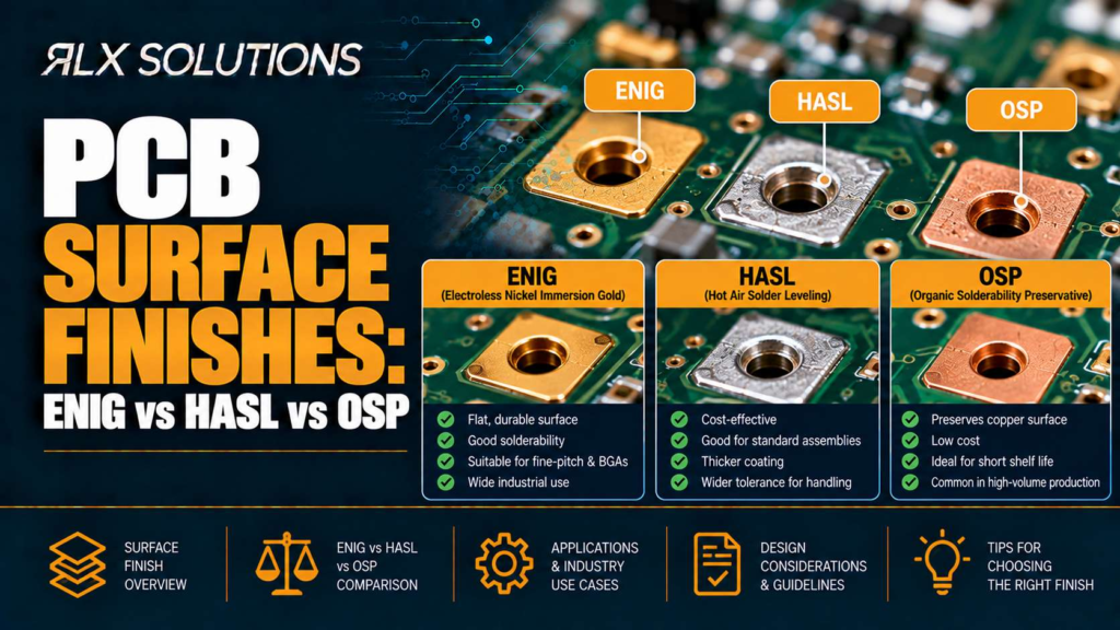
ENIG, HASL and OSP protect exposed PCB copper before assembly, but they create different pad surfaces and process constraints. ENIG is flat and well suited to fine-pitch assembly, HASL is a practical solder-coated finish, and OSP uses a thin organic coating suited to controlled single-reflow builds. RLX Solutions reviews finish selection against the complete circuit board design.
| Decision factor | ENIG | HASL | OSP |
|---|---|---|---|
| Finished pad | Nickel with thin immersion gold | Solder-coated copper | Organic coating over copper |
| Pad flatness | High | Lower because solder thickness varies | High |
| Fine-pitch suitability | Strong | Geometry can become the limiting factor | Flat surface supports placement |
| Reflow consideration | Suitable where multiple assembly operations are planned | Common solderable finish | Best treated as a single-reflow choice |
| Handling sensitivity | Gold protects the nickel surface | Solder coating protects exposed copper | Surface condition depends more heavily on handling and process control |
| Main engineering reason to choose it | Flat pads and predictable contact surface | Straightforward solder-coated finish | Minimal deposited metal and flat pads |
| Main reason to reconsider it | Added finish process compared with simpler alternatives | Pad coplanarity on small features | Reflow exposure and handling requirements |
ENIG gives fine-pitch components a flatter landing surface
Electroless nickel immersion gold (ENIG) deposits nickel over the exposed copper and then a thin immersion-gold layer over the nickel. The nickel acts as the primary barrier and solderable surface beneath the gold, while the gold protects it before assembly. For the full picture, see our PCB Manufacturing Guide.
For an ENIG printed circuit board, the important assembly advantage is geometry. The finish follows the pad rather than leaving a solder coating with the height variation associated with HASL. That matters as component pitch and pad area decrease.
Consider an 8-layer, 1.6 mm board carrying a 0.5 mm-pitch ball grid array (BGA). If the BGA escape routing and solder-mask geometry are already consuming most of the available layout margin, adding avoidable pad-height variation works against placement and solder-paste control. ENIG preserves a flat pad surface, so the assembly process starts with more consistent component landing geometry.
The finish does not fix poor footprint design. Paste volume, solder-mask openings, stencil design, placement, reflow and inspection still determine the assembled joint. For BGA, land grid array (LGA) and quad flat no-lead (QFN) packages, post-reflow automated optical inspection (AOI) may also be supplemented by X-ray where joints cannot be inspected optically.
ENIG also changes what must be controlled during fabrication. Nickel and gold deposition are chemical processes, so bath control and surface preparation matter. Finish selection should therefore be part of the fabrication specification rather than an assembly decision made after the bare board design is complete.
For reference, an ENIG build can use a nickel thickness of 3 to 6 µm with 0.05 to 0.1 µm of gold. Those layers should be treated as part of the finished pad system, not as decorative gold plating.
HASL works differently because the solder itself forms the finish
Hot air solder levelling (HASL) coats exposed copper with solder and removes excess solder with hot air. Lead-free HASL can use SnCuNi solder, while tin-lead HASL remains a separate finish option.
The manufacturing mechanism explains both the attraction and the limitation. HASL leaves a directly solderable metallic coating, but the levelling process does not create the same planar pad surface as ENIG or OSP. On larger pads and less demanding component geometries, that distinction may have little practical effect. On dense fine-pitch footprints, it can become part of the assembly tolerance stack.
Take a 4-layer, 1.6 mm control board using 0603 passives, SOIC packages and through-hole connectors. The design does not depend on extremely small, closely spaced landing surfaces. A HASL finish can fit the assembly geometry without forcing the designer to optimise every pad for maximum coplanarity.
Now replace the central device with a 0.4 mm-pitch package while keeping the board outline and layer count unchanged. The surface-finish decision deserves another review. The question is no longer whether HASL is solderable. It is whether the finished pad geometry leaves enough process margin for paste printing, placement and reflow on the smaller footprint.
That distinction prevents a common specification error: choosing a finish by board layer count. A 2-layer PCB can have demanding fine-pitch assembly, while a 12-layer circuit board can carry relatively forgiving packages. Component geometry, assembly sequence and exposed-contact requirements can matter more to the finish decision than the number of copper layers.
OSP removes deposited metal from the pad stack
Organic solderability preservative (OSP) protects exposed copper with an organic film rather than adding a nickel-gold or solder coating. The result is a flat surface because the finish does not build a comparatively thick metallic layer over the pad.
That makes OSP attractive where pad planarity matters, but its process window must match the assembly plan. OSP should be specified with the expected thermal exposure in mind, and it is suited to single-reflow builds.
Imagine a 6-layer, 1.2 mm board with 0.5 mm-pitch components on the top side and no second reflow operation planned. OSP can provide the flat pad geometry needed for placement without adding a nickel-gold finish.
Change that same board so the manufacturing plan requires additional thermal cycles or a more complicated two-sided assembly sequence. Surface finish is now linked directly to the process route. A finish that works for the original single-reflow design should not automatically carry over to the revised assembly flow.
Handling also becomes more significant because the protected copper surface must remain suitable for soldering through fabrication, storage and assembly. The finish cannot be evaluated separately from packaging, board handling and the time between fabrication and soldering.
Board A vs Board B shows why identical layer counts can price differently
Surface finish is one manufacturing variable among several. Two boards with the same layer count can require substantially different fabrication and assembly routes because finish, via structure and component geometry change the number and type of processes involved.
Consider these hypothetical 10-layer boards:
| Design feature | Board A | Board B |
|---|---|---|
| Layer count | 10 | 10 |
| Board thickness | 1.6 mm | 1.6 mm |
| Surface finish | Lead-free HASL | ENIG |
| Smallest assembly pitch | 0.8 mm | 0.4 mm |
| Via structure | Through-hole vias | Layer 1 to Layer 2 microvias plus through vias |
| Small via geometry | 0.20 mm mechanical hole | 0.10 mm laser microvia |
| Via-in-pad | No | Filled, capped and planarized on selected pads |
| Primary manufacturing concern | Conventional plated-hole and solder-finish processing | Fine-pitch pad geometry plus HDI processing |
Board B does not become more involved because ENIG alone makes it so. Its 0.4 mm-pitch package, laser-drilled Layer 1 to Layer 2 microvias and filled, capped via-in-pad structure introduce fabrication stages that Board A does not require.
Via-in-pad illustrates the interaction particularly well. When a via is placed directly inside a component pad, leaving the hole open can allow solder to move into the via during assembly. Resin filling, copper capping and planarization turn that location back into a usable component landing surface. A flat surface finish then sits on top of an already planarized structure.
This is why comparing PCB quotations by layer count and finish name alone can be misleading. The manufacturer needs the stackup, drill structure, Gerbers or equivalent manufacturing data, and assembly information to understand what the finish is actually being asked to support.
Choose the finish from the assembly constraints backwards
Start with the component and process condition that has the least margin. The finish decision becomes clearer once that constraint is identified.
- Choose ENIG when pad flatness is a major design requirement. Fine-pitch BGA, LGA and QFN footprints are strong reasons to examine ENIG because their assembly geometry benefits from a planar surface.
- Consider HASL when the component geometry tolerates its surface profile. Larger-pitch packages, through-hole parts and less demanding surface-mount footprints may not justify choosing a flatter finish solely for planarity.
- Use OSP when its flat copper surface and assembly route fit a controlled single-reflow build. Treat the reflow plan as part of the finish specification rather than assuming the same finish can follow every assembly sequence.
- Check whether the board has exposed contacts that impose another requirement. Connector fingers are mechanically different from ordinary solder pads. Hard gold with edge beveling can be used for gold-finger applications because repeated contact changes the surface requirement.
- Review the finish with via-in-pad and HDI geometry. Filled and capped vias, microvias and dense BGA escape structures change the pad system beneath the finish.
This approach also separates surface finish from solderability as a single-variable problem. A solderable finish cannot compensate for poor paste printing, unsuitable stencil apertures, incorrect component storage or a reflow profile that does not fit the assembly.
Surface finish affects inspection, but it does not replace inspection
The finish establishes the surface presented to the assembly process. Inspection determines whether that process produced the required result.
Solder paste inspection (SPI) before reflow can detect paste-volume, area and offset problems before components are permanently soldered. AOI after reflow can identify visible placement and solder-joint defects. BGA, LGA and QFN thermal-pad joints may require X-ray because the critical solder interfaces are hidden beneath the package.
Consider a 6-layer ENIG board with a 0.5 mm-pitch BGA. ENIG can provide flat pads, but it cannot reveal a bridge or insufficient solder beneath the installed package. The assembly inspection plan still needs a method capable of seeing the relevant joint.
The same principle applies to HASL and OSP. Finish selection controls the starting surface. Assembly process control and inspection determine whether that surface becomes an acceptable soldered connection.
Treat surface finish as part of the fabrication package
A manufacturer should not have to infer ENIG, HASL or OSP from component type. Put the required finish in the fabrication documentation and keep it consistent across the released manufacturing files.
The finish should be reviewed alongside the stackup, copper geometry, solder-mask openings, drill data and assembly requirements. If controlled impedance, fine-line routing, microvias or via-in-pad are present, those features may have a greater manufacturing impact than the finish itself.
For example, specifying ENIG on a conventional 4-layer board with 1 oz outer copper and 6 mil routing is a different manufacturing problem from specifying ENIG on an HDI board containing 0.10 mm laser microvias and filled, capped via-in-pad features. The finish name is identical. The process underneath it is not.
That is also why surface-finish substitutions should receive engineering review. Changing from one finish to another changes more than a line on a purchase order. It can alter pad geometry, assembly assumptions and the manufacturing sequence used to prepare the exposed copper.
Put ENIG, HASL and OSP into the DFM review
If you are releasing a new PCB or changing the finish on an existing design, RLX can review the choice against the stackup, component geometry and assembly route as part of the engineer-reviewed design for manufacturability (DFM) process. Send the complete manufacturing package so the finish can be evaluated in the context of the board rather than as an isolated specification.
FAQ
Is ENIG better than HASL for fine-pitch components?
ENIG provides a flatter finished pad than HASL, which is useful as package pitch decreases and placement geometry becomes less forgiving. That does not make ENIG universally preferable. A board populated with larger-pitch surface-mount and through-hole parts may not receive the same practical benefit from the flatter surface.
Can OSP be used on a fine-pitch PCB?
OSP produces a flat surface because it protects the copper with an organic coating rather than a deposited solder layer. That geometry can suit fine-pitch placement. The assembly route still matters, however. OSP should be considered with the expected reflow exposure and handling conditions, and it is suited to controlled single-reflow builds.
Is lead-free HASL different from tin-lead HASL?
Yes. They are separate solder-finish systems. Lead-free HASL can use SnCuNi solder, while tin-lead HASL uses a tin-lead alloy. If product compliance requirements restrict lead, the finish specification needs to state the required system clearly rather than using “HASL” alone and leaving the alloy open to interpretation.
Should gold fingers use ENIG?
Connector fingers have a different mechanical requirement from ordinary solder pads because the contact surface can experience repeated insertion and wear. Hard gold is available specifically for gold-finger applications, including 30 µ″ and 50 µ″ options with beveling. The connector requirement should therefore be specified separately rather than assuming the board’s general ENIG finish covers it.
What files are needed to quote a PCB with a specified surface finish?
For bare-board fabrication, manufacturing data can include Gerber RS-274X, ODB++, IPC-2581 files and NC drill data, plus relevant stackup and fabrication documentation. Assembly quotations also need the bill of materials, pick-and-place or centroid data and assembly drawing. Complete files allow finish selection to be reviewed against the actual board geometry.