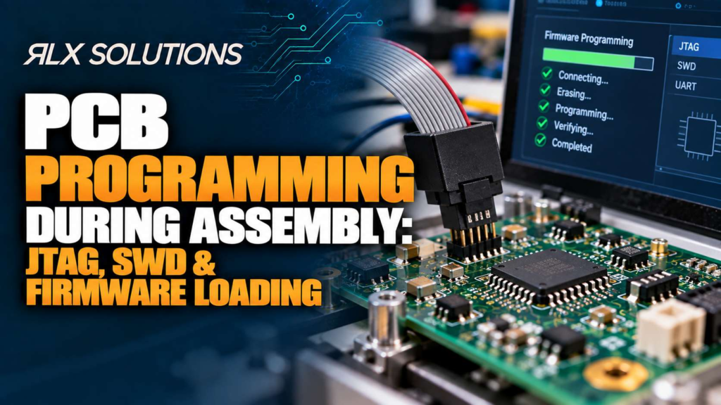
PCB programming during assembly loads firmware after components are placed, giving manufacturers a controlled point to verify communication, assign device data and prepare the circuit board for functional test. RLX Solutions, a contract electronics manufacturer in Concord, Ontario, supports in-system programming through JTAG, SWD, bootloader and firmware flashing as part of assembly.
Programming Is a Manufacturing Operation, Not Just a Firmware Task
Programming looks simple from the software side: connect to a target, load an image and confirm success. On an assembly line, each of those actions depends on hardware access, power sequencing, fixture contact, firmware revision control and traceability.
In-system programming (ISP) means loading code into a device while that device is already installed on the assembled printed circuit board. The advantage is straightforward. The manufacturer does not need every programmable component to arrive pre-programmed, and the board can be programmed closer to the point where its hardware is ready to be tested.
That also changes where failures appear. A programming station can expose an assembly defect before functional test. If a microcontroller cannot be identified through Serial Wire Debug (SWD), the cause might be the programming image, but it might also be a soldering fault, incorrect component, missing supply rail, reset-state problem or poor fixture contact.
The useful manufacturing question is therefore not simply, “Can this device be programmed?” It is, “Can every assembled board be programmed repeatably, verified and associated with the correct production record?”
Programming belongs in the process flow
- Assemble the circuit board.
- Inspect solder paste and component placement through the specified inspection stages.
- Establish controlled electrical contact with the programming interface.
- Power the target in the required state.
- Identify the target device.
- Load the approved firmware image.
- Verify the programmed contents or programmed state.
- Apply required serialization or device-specific data.
- Run functional test to the customer’s specification.
- Log pass/fail information against the serialized unit.
That separation between programming and functional test matters. Successful flashing proves that a defined programming transaction completed. It does not prove that every circuit on the board functions correctly.
JTAG, SWD and Bootloader Programming Solve Different Access Problems
Joint Test Action Group (JTAG), SWD and bootloader-based flashing can all place firmware onto assembled hardware, but they reach the target differently. The interface choice affects PCB layout, fixture design, production access and recovery when something fails.
| Decision factor | JTAG | SWD | Bootloader |
|---|---|---|---|
| Physical interface | Dedicated debug/test signals | Compact debug interface | Device-dependent communication interface |
| Typical target | Devices supporting JTAG access | SWD-capable microcontrollers | Devices with a suitable boot mechanism |
| Board access requirement | Test or connector access to required signals | Access to SWD signals, power reference and supporting control signals as required | Access to the boot communication path and required boot-state controls |
| Production concern | Signal access and chain configuration | Reliable contact and target state | Boot configuration and communication availability |
| Recovery planning | Depends on target and board architecture | Depends on target and board architecture | Depends strongly on boot path remaining accessible |
JTAG is more than a generic connector name. It is an access architecture that can support device communication and, depending on the design, multiple devices in a chain. The manufacturing problem becomes more involved when one board contains several programmable targets because chain configuration, device order and access conditions must match the programming setup.
SWD uses a smaller signal set for supported microcontrollers. That can make physical access easier on dense designs, but reducing the number of interface signals does not eliminate the manufacturing requirements. The fixture still needs dependable contact, a stable electrical reference and a target that enters the expected state.
Bootloader flashing uses firmware already present in the device to receive another image over a supported communication path. This can reduce reliance on a dedicated debug connection in some architectures, but the bootloader itself becomes part of the programming dependency. Boot-state configuration and the selected communication interface must work before the application image can be loaded.
Worked example: the same controller, two production-access strategies
Consider a hypothetical 6-layer board using a 0.5 mm-pitch microcontroller. The PCB is 1.6 mm thick, and the application image is loaded after surface-mount assembly.
Board A routes its SWD programming signals, reset and electrical reference to accessible test pads on the underside. A production fixture can contact those points while the assembled board is powered in a defined programming state.
Board B uses the same 6-layer stackup and controller but leaves programming access only on a small development connector that becomes obstructed after the product is mechanically assembled.
The firmware image may be identical. The manufacturing problem is not. Board A was laid out around repeatable production contact. Board B creates a process dependency on when the housing is installed and whether an operator can still reach the connector.
That difference can affect fixture design, work sequence, reprogramming access and fault recovery without changing the layer count or firmware at all.
Design Programming Access Before the PCB Layout Is Released
Programming should influence the circuit board before manufacturing files are frozen. A firmware-loading requirement discovered after layout can force hand access, temporary wiring or a fixture that has to reach pads never intended for production probing.
The manufacturer needs a defined electrical path to the programmable device. That usually means considering programming signals, ground reference, target power, reset behaviour and any pins that determine boot mode.
Physical placement matters too. A perfectly routed programming pad is of little production value if a tall connector, shield, heat sink or enclosure blocks the probe.
Test pads also have to survive the actual contact method. A development engineer may touch a board once with a bench probe. Production equipment may contact the same location repeatedly across a lot. Pad geometry, spacing and surrounding component clearance therefore become manufacturing inputs rather than cosmetic layout decisions.
Keep programming and test access from fighting each other
The same underside of a PCB may need programming probes, flying-probe access or a bed-of-nails in-circuit test (ICT) fixture. Programming points cannot be considered in isolation from the rest of the test strategy.
For prototype and low-volume assembly, flying-probe ICT can provide full-net coverage without a dedicated fixture. At production volume, bed-of-nails ICT may use a customer-supplied or manufacturer-developed fixture. Functional test (FCT) then exercises the board to the customer’s specification and can log pass/fail results with serial traceability.
Planning these operations together can prevent a late-stage fixture problem in which the most convenient programming pad is inaccessible because another mechanical or electrical requirement occupies the same area.
Firmware Release Control Prevents the Wrong Code From Becoming a Good Board
A programming station can execute perfectly and still produce the wrong product if it receives the wrong image.
Manufacturing therefore needs an unambiguous relationship between the hardware being assembled and the firmware approved for it. File names such as final.bin, latest.hex or production_new.bin do not establish that relationship.
The production package should identify the firmware image, target device, applicable hardware revision, programming method and any device-specific configuration required by the build. If multiple variants share one circuit board, the manufacturing instructions also need a way to distinguish which image belongs to which assembly.
Consider a hypothetical product family using the same 8-layer PCB and the same microcontroller. Variant X receives firmware revision 3.4 and Variant Y receives revision 3.7 because the two products use different sensor configurations. Electrically, both images may flash successfully onto both boards.
That is precisely why programming success cannot serve as variant verification. The manufacturing process needs a separate control linking the assembly identity to the approved image before flashing starts.
Board A vs Board B: Why Equal Layer Counts Can Produce Different Programming Costs
Layer count is a poor proxy for programming effort. Two 10-layer circuit boards can require very different production processes even when their bare PCB construction is comparable.
| Decision factor | Board A | Board B |
|---|---|---|
| PCB construction | 10 layers, 1.6 mm thick | 10 layers, 1.6 mm thick |
| Programmable targets | One MCU | MCU plus FPGA |
| Programming access | Dedicated SWD pads | SWD plus JTAG access |
| Firmware variants | One | Three product variants |
| Unit identity | Serial number only | Serial number plus programmed device data |
| Production verification | Firmware load followed by FCT | Multiple programming operations followed by FCT |
| Main process risk | Fixture contact or target-state failure | Wrong target, wrong image or incorrect identity mapping |
Board A requires one controlled programming transaction. Board B adds another programmable target and multiple image-selection conditions. That means more manufacturing logic even though both boards have ten layers.
The cost mechanism is process content. Each additional target or variant can add file control, target selection, contact requirements, verification steps and failure paths. Procurement teams comparing assembly quotations should therefore describe the programming workflow rather than assuming firmware loading is a single line item determined by PCB complexity.
Programming Failures Need to Be Separated From Assembly Failures
A failed programming attempt is a symptom, not a diagnosis.
Suppose a hypothetical 4-layer, 1.2 mm-thick board uses SWD to program a microcontroller after reflow. The programmer cannot identify the target. Repeating the flash command five times does not establish whether the firmware is at fault.
The failure path may begin with several distinct conditions:
- The target is not receiving the expected supply.
- Reset is held in the wrong state.
- A programming signal has an open or short.
- The installed device is incorrect.
- Fixture probes are not contacting the pads.
- Boot configuration prevents the expected access path.
- The programming setup does not match the target or approved image.
Inspection and electrical test help narrow that tree. Solder paste inspection (SPI) checks paste volume, area and offset before reflow. Automated optical inspection (AOI) checks the assembled board after reflow. Automated X-ray inspection (AXI) can examine hidden joints on packages such as BGA, LGA and QFN devices. Those operations answer different questions from firmware flashing.
This distinction becomes particularly useful with hidden-joint packages. If a 0.4 mm-pitch BGA device communicates intermittently during programming, a software retry policy should not become a substitute for investigating power, connectivity and solder-joint integrity.
Serialization Turns Firmware Loading Into a Traceability Operation
Programming can write more than executable firmware. Some products also require unit-specific data such as serial information or a media access control (MAC) address.
Once unique data is written, programming becomes part of product identity control. The manufacturing record has to preserve the relationship between the physical unit, programmed data and subsequent test result.
Serialization can be represented physically by serial marking, a laser mark or a label, while electronic identity can be programmed into the assembly where the product architecture requires it. The important manufacturing principle is one-to-one association.
A duplicate identifier can create a product that passes electrical test yet fails later at provisioning, service or network deployment. A missing association between programmed identity and test result can also weaken failure analysis because the production record no longer tells you exactly which unit received which data.
Functional testing to the customer’s specification can provide pass/fail logging with serial traceability. That makes the transition from programming to FCT an important control point: the unit that was just flashed must remain associated with the correct record as it moves through test.
First Article Approval Is Where the Programming Process Gets Proven
The first article should prove more than component placement. For a new build involving firmware loading, it is also the point to confirm that the production process can reach the target, apply the intended image and hand the board into the required test flow.
First article inspection (FAI) before production lot release creates a useful boundary between setup and repeated manufacturing. A programming problem discovered here is fundamentally different from one discovered after a full production lot has been assembled.
For example, consider a hypothetical mixed-technology board with an 8-layer PCB, a 0.5 mm-pitch microcontroller and an SWD programming interface. The first article flashes successfully on the bench, but the planned production fixture cannot contact one pad because a through-hole connector body overhangs it after insertion.
The firmware is valid and the board is electrically programmable. The process is still not production-ready.
That example also shows why assembly sequence matters. Programming before the connector is inserted might restore access, but that choice must fit the wider manufacturing and test sequence rather than becoming an undocumented workaround.
Give the Manufacturer a Programming Package That Can Be Executed Without Guessing
A complete PCB assembly package already needs the bill of materials (BOM), pick-and-place or centroid data and assembly drawing. Programming adds another set of controlled inputs.
For a firmware-loading build, the production instructions should make the intended transaction clear: which target is programmed, which approved image belongs to the assembly, how the target is accessed, what hardware state is required, what verification defines success and whether unit-specific data must be written.
The circuit board files matter as well. Manufacturing data can be supplied as Gerber RS-274X, ODB++, IPC-2581 and NC drill files, with supporting stackup, impedance and assembly documentation where applicable.
Do not leave production programming requirements trapped in an engineer’s bench setup. A programmer executable, a cable and someone’s memory of the reset sequence are not a manufacturing definition.
The stronger handoff is one another engineer can reproduce from controlled files and instructions.
Treat Firmware, Inspection and Functional Test as One Production System
Programming is most useful when it sits between known assembly quality and known functional performance.
Inspection can establish whether manufacturing conditions and component placement meet the build requirements. Programming can establish communication with the target and load the approved image. FCT can then exercise the completed assembly against the customer’s specified behaviour.
Those stages catch different defect classes. Combining them does not mean treating them as interchangeable.
A board that passes AOI can still fail programming because the target is electrically inaccessible. A board that programs successfully can still fail FCT because an analogue channel, peripheral, connector or power function does not perform correctly. A board that passes both can still have a traceability problem if the programmed identity was not associated with the production record.
That is why firmware loading belongs inside the manufacturing plan rather than being treated as an informal step after assembly.
Put Programming Requirements Into the Quote Package
If your circuit board needs JTAG, SWD, bootloader flashing, serialization or firmware loading, define those requirements before the assembly process is released. RLX can review programming requirements alongside the assembly package, engineer-reviewed DFM, inspection and customer-specified functional test so that production access and verification are considered before the lot moves forward.
FAQ
Can firmware be loaded after the components are soldered to the PCB?
Yes. In-system programming allows firmware to be loaded into supported devices after they are mounted on the assembled PCB. The board still needs suitable electrical access and the target must be placed in the required programming state. JTAG, SWD, bootloader and firmware flashing can all be incorporated into an assembly process when the hardware and programming instructions support them.
Is successful JTAG or SWD programming the same as a functional test?
No. Successful programming confirms that the intended programming transaction completed under the defined process. Functional testing checks board behaviour against the customer’s test specification. A microcontroller can accept firmware even when another circuit on the assembly has a defect, so programming and FCT should be treated as separate manufacturing controls.
What files should I provide for PCB assembly with firmware programming?
For assembly, provide the BOM, pick-and-place or centroid file and assembly drawing along with the applicable manufacturing files. Programming also requires the approved firmware image and clear instructions identifying the target and required programming operation. Where the product uses variants or serialized data, the package should also define how the correct image or identity maps to each assembly.
Can serial numbers or MAC addresses be programmed during assembly?
Yes. Serialization can include serial marking, MAC address programming, laser marking or labels. When electronic identity is written during manufacturing, the process should preserve the association between that data and the physical unit. Functional testing can then log pass/fail information with serial traceability when that requirement is included in the customer’s test specification.
Should programming pads be included in the PCB layout?
If production programming requires direct electrical access, the layout should provide access compatible with the planned programming method and manufacturing sequence. Placement matters as much as connectivity because connectors, shields, heat sinks or mechanical hardware can obstruct otherwise usable pads. Programming access should therefore be reviewed alongside assembly, inspection and test access before layout release.
Can programming problems be caught during first article inspection?
The first article provides an early point to verify that the new build can move through its intended manufacturing process before production lot release. For a programmed assembly, that can expose practical issues such as inaccessible programming points, incorrect process sequencing or a mismatch between the production setup and the supplied programming requirements.