SMT assembly is the process of printing solder paste, placing surface-mount components, reflowing the solder, and inspecting and testing the finished circuit board. RLX Solutions, a contract electronics manufacturer in Concord, Ontario, approaches SMT assembly as a controlled manufacturing sequence in which PCB design, component condition, paste deposition, placement and thermal processing all affect yield.
SMT Assembly Starts Before the Placement Machine
Surface-mount technology (SMT) attaches components directly to pads on the surface of a printed circuit board rather than routing every connection through a drilled hole. That changes assembly from a manual insertion problem into a coordinated printing, placement and thermal process. For the full picture, see our PCB Assembly Guide.
The manufacturing sequence may look linear, but the decisions are connected. A pad geometry affects paste transfer. Paste volume affects solder joint formation. Package type determines whether optical inspection can see the finished connection. Component moisture condition can influence what happens during reflow.
Before production begins, the assembler needs enough information to connect those decisions correctly. For a typical SMT build, that means:
- Bill of materials (BOM): identifies manufacturer part numbers, quantities and approved component selections.
- Pick-and-place or centroid file: provides each component’s board position, rotation and reference designator.
- Assembly drawing: resolves polarity, orientation, special placement instructions and build notes.
- PCB manufacturing data: establishes the pad pattern, solder mask openings, board outline and other physical features.
- Test requirements: define what must be electrically or functionally verified after assembly.
An engineer-reviewed design for manufacturability (DFM) and design for assembly (DFA) review should happen before material reaches the line. Discovering an incorrect footprint after components have been loaded into feeders is much more expensive than resolving it from the source files.
Step 1: Bare PCB Condition Sets the Starting Point
SMT cannot compensate for a poor bare board. Pad geometry, solder mask registration, board flatness and surface finish all influence how consistently solder paste prints and how components behave during reflow.
A bare PCB is the fabricated circuit board before components are installed. Once parts are soldered onto it, the assembly is commonly called a printed circuit board assembly, or PCBA.
Surface finish matters because the component terminal is not soldering directly to exposed base copper. The finish protects the pad before assembly and becomes part of the soldering interface.
Available board finishes can include HASL, ENIG, ENEPIG, immersion silver, immersion tin and OSP. The choice should account for component pitch, storage and handling requirements, soldering sequence and any downstream process such as wire bonding or edge-connector use.
Solder mask also enters the assembly equation. Fine-pitch packages leave less room between adjacent pads, so mask geometry and registration become part of the solder-bridge risk rather than a cosmetic board detail.
Step 2: Solder Paste Printing Controls the First Physical Variable
Solder paste is a mixture of metal alloy particles and flux deposited on PCB pads before component placement. A stencil controls where the paste lands and how much is transferred.
Printing errors can propagate through every later operation. A placement machine can put a component exactly where the centroid file says, yet the joint can still fail if the paste deposit underneath it is incomplete, excessive or shifted.
The printer therefore has to control several interacting variables:
- Stencil-to-board registration
- Aperture geometry
- Paste condition
- Board support
- Squeegee motion
- Stencil release
- Cleaning frequency
Solder paste inspection (SPI) checks the print before components are placed. The inspection measures paste volume, area and offset, which makes it possible to identify a printing problem while the board can still be cleaned and reprinted rather than after components have passed through reflow.
Worked Example: One Package Creates Two Paste Problems
Consider a hypothetical 8-layer, 1.2 mm thick circuit board using 01005 decoupling capacitors around a 0.4 mm-pitch QFN with an exposed thermal pad.
The small passive pads require repeatable paste transfer at very small geometries. The QFN thermal pad creates the opposite concern: one large central deposit can place too much solder beneath the package.
If excessive paste lifts the QFN body, the perimeter terminations may not form as intended. If transfer to the 01005 pads is inconsistent, the same board can develop opens or component movement elsewhere.
That is why stencil design and SPI belong to the same process discussion. The assembler needs to know whether the defect originated during paste transfer before adjusting placement or reflow settings that were never the actual cause.
Step 3: Pick-and-Place Converts Design Coordinates Into Physical Parts
Pick-and-place equipment takes components from reels, trays, tubes or other feeders and places them onto printed solder paste according to the centroid data.
A component’s X and Y coordinates are only part of the problem. The machine also needs the correct rotation, package definition, feeder assignment, pickup method and placement sequence.
Polarity-sensitive devices add another failure path. Diodes, light-emitting diodes, polarized capacitors and integrated circuits can be positioned accurately but electrically backwards if the BOM, footprint library, assembly drawing and component marking do not agree.
Fine-pitch packages also reduce the margin for data errors. SMT assembly can include passives as small as 01005 and ball grid array (BGA) packages down to 0.3 mm pitch. At that scale, a questionable library origin or rotation convention should be resolved in the manufacturing data rather than interpreted at the machine.
Placement sequencing matters as well. Larger or heavier components may behave differently from small passives as the populated board moves toward reflow. On double-sided assemblies, the process has to account for components that will experience more than one thermal cycle.
Step 4: Reflow Creates the Solder Joint
Reflow soldering heats the populated PCB through a controlled thermal profile until the solder paste activates, melts and forms joints between component terminations and board pads.
The profile has to satisfy competing thermal conditions across the same circuit board. Small passive components heat quickly. Large copper regions, connectors, shields and power components can absorb more energy.
That difference is why the board’s copper distribution matters to assembly even though copper is defined during PCB layout and fabrication.
If heating is poorly balanced, several failure modes can appear. Small components can move as solder wets unevenly. Flux activation can be mistimed. Large joints may not form as expected. Packages and boards also experience mechanical stress as materials with different coefficients of thermal expansion heat and cool.
A reflow issue therefore should not automatically be treated as an oven-setting issue. The root cause can begin with pad design, paste volume, component storage, copper distribution or part geometry.
Step 5: Inspection Has to Match the Component Package
No single inspection method sees every SMT defect. The correct inspection flow changes with the package because some solder joints remain visible after reflow and others are hidden underneath the component body.
Automated optical inspection (AOI) uses imaging to examine visible assembly conditions after soldering. It is effective for issues such as component presence, orientation, positional errors and visible solder-joint conditions. Post-reflow AOI can be performed on both sides of the assembly.
BGA, land grid array (LGA) and some quad flat no-lead (QFN) connections create a different problem. Their critical solder interfaces can sit beneath the component, outside direct optical view.
Automated X-ray inspection (AXI) provides visibility into those hidden structures and can be used for BGA, LGA, QFN thermal pads and void analysis.
Manual visual inspection under magnification remains part of the process as well, with workmanship evaluated to IPC-A-610 Class 2 or Class 3 requirements as specified for the build.
Inspection depth should therefore follow the assembly architecture. Adding a hidden-joint package changes the inspection plan even if the PCB itself has not gained a single layer.
Same PCB Layer Count Does Not Mean the Same SMT Assembly Cost
PCB layer count is a poor shortcut for estimating assembly effort. Two boards with the same six copper layers can require very different SMT manufacturing sequences.
Consider these two hypothetical designs:
| Decision Factor | Board A | Board B |
|---|---|---|
| PCB construction | 6 layers, 1.6 mm | 6 layers, 1.6 mm |
| Assembly sides | Top side only | Top and bottom |
| Smallest passive | 0402 | 01005 |
| Area-array package | None | 0.3 mm-pitch BGA |
| Hidden solder joints | No | Yes |
| Paste/place cycles | One | Two |
| Reflow exposure | One assembly cycle | Double-sided process |
| Primary inspection | AOI and visual | AOI, visual and X-ray |
Board B can cost more to assemble even though the bare PCB layer count and thickness are identical.
The mechanism is manufacturing content. A second populated side adds another print and placement sequence. The 01005 parts tighten printing and placement control. The BGA introduces hidden solder joints that call for X-ray inspection. More feeder positions and more placements can increase setup and machine time.
This distinction matters during cost reduction. Removing two PCB layers may have less impact on assembly cost than reducing part count, consolidating package types or moving components to one side when the electrical and thermal design allows it.
SMT Components Change the Process Around Them
“Surface-mount component” covers a wide range of mechanical and thermal behaviours. The package determines how the part is fed, picked up, aligned, soldered and inspected.
| Component Type | Assembly Consideration |
|---|---|
| Chip resistors and capacitors | Pad symmetry and paste consistency affect movement during reflow |
| SOT and similar discrete packages | Orientation and terminal wetting remain visually accessible |
| Gull-wing ICs | Lead coplanarity, paste control and bridge detection matter as pitch decreases |
| QFN and LGA packages | Hidden or partly hidden joints increase dependence on paste control and X-ray |
| BGA packages | Solder joints sit beneath the package, making X-ray part of defect analysis |
| Large power components | Thermal mass and copper connection can alter local heating behaviour |
| Connectors | Mechanical loading and mixed SMT/through-hole construction may change the process route |
Mixed-technology boards can combine SMT with through-hole components. In those builds, SMT reflow may be followed by operations such as selective soldering, press-fit insertion or other secondary assembly steps.
The assembly drawing should make that sequence unambiguous. The manufacturer needs to know which components must survive later thermal or mechanical operations before selecting the process order.
Component Sourcing Is Part of SMT Process Control
The placement machine cannot correct a component authenticity, packaging or moisture problem.
Turnkey SMT assembly places procurement under the manufacturer’s scope. A kitted or partial-turnkey build divides purchasing responsibility between customer and manufacturer. In a consigned build, the customer supplies the complete kit.
Whichever model is used, component condition matters when the parts reach production.
Moisture-sensitive devices require controlled storage and handling under IPC/JEDEC J-STD-033 practices. Electrostatic-sensitive devices need controlled handling in ANSI/ESD S20.20-aligned protected work areas.
Sourcing risk increases further when a required component is obsolete, allocated or unavailable through normal authorized channels. Counterfeit-prevention controls can then extend beyond checking a label. Packaging integrity, date and country-of-origin information, visual inspection, lot verification, X-ray and electrical testing may all become part of the verification path. Higher-risk cases can escalate to decapsulation and die analysis.
The practical design lesson is simple: an electrically valid BOM can still be difficult to manufacture if its sourcing assumptions are weak.
Step 6: Electrical Test Finds Defects Inspection Cannot Prove
Inspection answers questions about the physical build. Electrical testing answers different questions about connectivity and operation.
Flying-probe in-circuit test (ICT) is useful for prototype and lower-volume assemblies because it can achieve net coverage without a dedicated fixture. Production programmes can use bed-of-nails ICT when a fixture is justified.
Functional test (FCT) goes beyond static connectivity by operating the assembly according to customer-defined requirements. Pass/fail results can be logged with serial traceability.
Those methods should not be treated as substitutes for AOI or X-ray. A solder joint can appear questionable but still pass an electrical test at one moment in time. Conversely, a visually acceptable assembly can fail because of an incorrect component value, programming problem or electrical fault that imaging cannot identify.
The test strategy is strongest when each method is assigned the defects it can actually detect.
Step 7: First Article Approval Protects the Production Lot
A first article inspection (FAI) checks the initial build before the main production lot is released. For a new assembly, customer sign-off provides a deliberate point to confirm that the physical product matches the approved documentation before more units move through the same process.
This is especially useful when the build combines several risk factors at once, such as fine-pitch SMT, polarized components, programming, serialization and functional test.
Suppose a hypothetical 10-layer, 1.6 mm board contains a 0.5 mm-pitch QFN, four BGAs, 600 total placements and a programmed microcontroller. AOI may confirm visible placement conditions, X-ray can examine the hidden BGA joints, and FCT can check defined board behaviour.
The FAI ties those separate checks back to one approved manufacturing configuration. If the firmware file or assembly drawing is wrong, finding that mismatch on the first approved unit prevents the same error from being repeated through the production lot.
Design for SMT Assembly Means Controlling Interactions
A manufacturable SMT design does not come from optimizing footprints, PCB fabrication and component sourcing independently. It comes from checking how they interact.
Before releasing the assembly package, review the design from several directions:
- Footprints versus actual packages: confirm land patterns, pin numbering and orientation against the selected components.
- BOM versus procurement: identify obsolete, allocated or high-risk parts before the build reaches purchasing.
- Pad geometry versus stencil printing: check whether fine-pitch and exposed-pad packages create competing paste requirements.
- Copper distribution versus reflow: consider whether large thermal regions sit next to low-mass components.
- Package style versus inspection: identify every connection that optical inspection cannot see.
- Assembly side versus process count: verify whether a second populated side is worth the additional manufacturing sequence.
- Test requirements versus board access: design test strategy while nodes and interfaces can still be made accessible.
- Programming versus traceability: specify firmware, serialization and pass/fail requirements in the released manufacturing package.
This is also where PCB fabrication and assembly need to stay connected. A decision such as via-in-pad can solve routing congestion around a dense BGA, but a plated-over filled via requires a different bare-board process before SMT starts. The assembly benefit depends on the fabricated pad arriving flat and suitable for paste printing.
Prepare the SMT Assembly Package Before You Request a Quote
An assembler can evaluate the job faster when the manufacturing package removes interpretation.
For an SMT build, provide the BOM in .xlsx or .csv format, pick-and-place data, assembly drawing and the PCB manufacturing files. Gerber RS-274X, ODB++, IPC-2581 and NC drill data can be used for the fabrication package, while a stackup PDF, impedance targets and fabrication notes provide additional board-level definition where applicable.
State the requested workmanship class, test requirements, programming requirements and any customer-supplied components at the same time.
Missing data often causes a commercial problem before it causes a manufacturing problem: two quotations may appear comparable even though the suppliers have priced different assumptions. A complete package gives engineering and purchasing a better basis for comparing scope.
From SMT Design Files to a Manufacturable Build
If you are preparing a new board for prototype or production, RLX includes engineer-reviewed DFM/DFA review with every quote. Send the Gerbers or other accepted PCB data, BOM, pick-and-place file and assembly drawing together so fabrication, component sourcing, placement, inspection and test requirements can be reviewed as one manufacturing package.
Frequently Asked Questions
What is the difference between SMT and through-hole assembly?
SMT places components directly onto pads on the surface of the printed circuit board. Through-hole assembly inserts component leads through drilled holes before soldering. Many products use both methods on the same assembly, with SMT handling dense electronic packages and through-hole or press-fit technology used where the component or mechanical requirement calls for it.
How small can components be for SMT assembly?
The assembly process can handle passive components down to 01005 and BGA packages with pitch down to 0.3 mm. Package size is only one part of manufacturability. Pad design, solder paste printing, component presentation, placement data, inspection access and the surrounding board layout also affect whether a dense assembly can be produced consistently.
Why is X-ray inspection used for BGA and QFN components?
Optical inspection cannot directly view solder joints hidden beneath a package. X-ray inspection provides information about structures below the component body, making it useful for BGA and LGA joints, QFN thermal pads and void analysis. AOI remains useful for visible conditions elsewhere on the same board, so the two inspection methods address different defect classes.
Does SMT assembly include component sourcing?
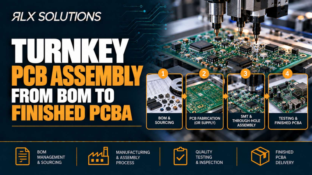
It can. A turnkey build can place component procurement, bare-board supply, assembly, inspection and test under one programme. Kitted builds allow the customer to supply selected critical or long-lead parts while the manufacturer sources the balance. Consigned assembly uses a complete customer-supplied kit. The correct model depends on who needs control of purchasing and inventory.
What files are needed for an SMT assembly quote?
Provide the PCB manufacturing data, BOM, pick-and-place or centroid file and assembly drawing. Include stackup information, impedance targets, fabrication notes, workmanship class, test requirements and programming instructions where they apply. Complete source data reduces assumptions during DFM/DFA review and makes the quoted manufacturing scope easier for engineering and procurement teams to evaluate.