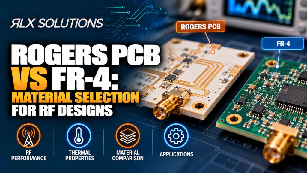
Rogers PCB materials generally make sense when RF performance depends on low dielectric loss, predictable impedance, or stable electrical behaviour across frequency and temperature. FR-4 remains practical when frequencies, trace lengths, and loss budgets leave enough margin. RLX Solutions, a contract electronics manufacturer in Concord, Ontario, reviews material selection against the complete RF stackup before fabrication.
Rogers PCB vs FR-4 at a glance
The practical difference is predictability. FR-4 describes a broad family of glass-reinforced epoxy laminates rather than one tightly defined RF material. Rogers high-frequency laminates are engineered around controlled electrical properties, making transmission-line behaviour easier to model when insertion loss and phase response matter. For the full picture, see our PCB Manufacturing Guide.
Dielectric constant, usually written Dk, describes how strongly the laminate affects the electric field and therefore transmission-line impedance and propagation velocity. Dissipation factor, or Df, represents dielectric energy loss. As frequency and electrical length increase, both properties become more important to the RF budget.
| Decision factor | FR-4 | Rogers high-frequency laminate |
|---|---|---|
| Primary advantage | Lower material and fabrication cost | More predictable RF electrical behaviour |
| Dielectric loss | Often acceptable for less demanding RF paths | Lower-loss grades available for RF and microwave circuits |
| Dk control | Depends strongly on the selected FR-4 system | Tightly characterized in RF laminate families |
| Impedance design | Practical when stackup and material data are controlled | Better suited to impedance-sensitive RF structures |
| Multilayer use | Straightforward | Can be used throughout a board or in hybrid constructions |
| Fabrication | Familiar conventional PCB processing | Process depends on the selected laminate family |
| Best fit | Cost-sensitive boards with sufficient RF margin | Loss-sensitive, phase-sensitive, microwave, antenna, and precision RF paths |
| Cost driver | Conventional material and process flow | Laminate, stackup construction, material handling, and process requirements |
The mistake is treating operating frequency as a single switching point. A 2.4 GHz circuit with a 10 mm RF path does not have the same material requirements as a 2.4 GHz board routing a weak signal through 180 mm of transmission line.
Electrical length, allowable insertion loss, impedance tolerance, temperature range, copper profile, geometry, and production repeatability all affect the decision.
Frequency alone does not decide between Rogers and FR-4
A material decision should start with the RF path rather than the number printed on the radio specification.
Consider a hypothetical four-layer 1.6 mm circuit board carrying a 2.4 GHz radio. The antenna feed runs 12 mm from the matching network to the antenna, with a continuous reference plane directly below it. If simulation and measurement show adequate margin, changing the whole PCB to a high-frequency laminate may add cost without solving a meaningful electrical problem.
Now keep the same 2.4 GHz frequency but extend the RF route to 160 mm through filters, connectors, and another RF stage. Dielectric and conductor losses accumulate over that distance. Material variability also has more physical length over which to affect phase and impedance.
That is why statements such as “FR-4 works below X GHz” are poor design rules. The more useful question is how much loss and variation the complete RF channel can tolerate.
Dielectric loss changes the RF power budget
Every real transmission line loses energy. Some loss comes from the conductor, some from the dielectric, and some from radiation or discontinuities.
A lower Df reduces the dielectric component of that loss. Rogers’ RO4003C, for example, is a low-loss high-frequency laminate, while the broader FR-4 category can cover materials with substantially different electrical characteristics. For an engineer, the important comparison is between the actual laminate data used in the field solver, not a generic “Rogers versus FR-4” assumption.
Copper matters at the same time. At high frequencies, current becomes increasingly concentrated near the conductor surface through skin effect. A rough copper interface increases the effective path travelled by that current and can increase conductor loss.
This creates an important design consequence: paying for a low-loss dielectric while ignoring copper profile can leave part of the expected insertion-loss improvement unrealized.
Worked example: same frequency, different loss exposure
Suppose Board A and Board B both operate at 6 GHz and use a 50 Ω transmission-line target.
Board A has a 15 mm RF route from an amplifier to a nearby connector. Board B has a 140 mm route crossing much of the printed circuit board before reaching its connector.
Even with identical layer count and nominal impedance, Board B has roughly nine times as much physical transmission-line length. That does not mean its total insertion loss is exactly nine times greater because transitions, conductor geometry, dielectric behaviour, and connectors also contribute. It does mean dielectric and conductor loss deserve much more weight in Board B’s material decision.
The channel budget should therefore be established before selecting the laminate.
Dk stability matters as much as the nominal Dk
Nominal dielectric constant tells you where to begin the impedance calculation. Variation tells you how closely manufactured boards can stay around that design point.
Characteristic impedance depends on conductor geometry and the surrounding dielectric system. Change the trace width, copper thickness, dielectric thickness, or Dk and the impedance changes with it.
This is why copying a 50 Ω trace width from a previous FR-4 board into a Rogers stackup is unsafe. A 0.25 mm trace that produced the intended impedance in one construction may not do so after the dielectric material or distance to the reference plane changes.
Controlled impedance therefore has to be treated as a stackup property, not a trace-width property.
For RF circuit boards, impedance verification also belongs in the manufacturing plan. Controlled impedance can be verified using a time-domain reflectometry (TDR) coupon, allowing the fabricated transmission-line structure to be checked against its target.
Hybrid Rogers and FR-4 stackups can put RF material where it matters
Choosing a Rogers laminate does not automatically mean every dielectric layer needs to use the same high-frequency material.
A hybrid stackup combines material systems so that RF-critical layers receive the electrical properties they need while less sensitive portions of the board use another laminate.
Consider an eight-layer board:
- Layer 1: RF components and controlled-impedance RF routing
- Layer 2: RF ground
- Layer 3: low-speed control signals
- Layer 4: power
- Layer 5: ground
- Layer 6: digital signals
- Layer 7: ground
- Layer 8: low-speed interfaces
If the sensitive RF structures are concentrated between Layers 1 and 2, the electrical case for using premium RF material throughout all eight layers may be weak. A hybrid construction can instead concentrate the material choice around the RF field structure.
But hybrid construction is not a free cost reduction. Different materials can have different dimensional, thermal, and bonding behaviour. The fabricator needs to establish the stackup as a complete construction rather than substituting dielectric sheets independently.
That discussion should happen before RF geometry is frozen.
Board A vs Board B: the same six layers can price differently
Layer count is a poor proxy for PCB manufacturing cost because it says nothing about material system or process sequence.
Take two hypothetical six-layer boards, each 1.6 mm thick and 100 mm × 80 mm.
| Factor | Board A | Board B |
|---|---|---|
| Layer count | 6 | 6 |
| Material approach | FR-4 construction | RF laminate used around critical RF layers |
| RF routing | Short 2.4 GHz antenna feed | Multiple 10 GHz controlled-impedance paths |
| Smallest mechanical hole | 0.30 mm | 0.30 mm |
| Via structure | Through vias | Through vias |
| Impedance requirement | One controlled RF feed | Multiple controlled RF structures |
| Material priority | Cost with adequate RF margin | Loss and electrical consistency |
| Manufacturing consequence | Conventional material construction | Material-specific stackup and RF process control |
Board B can cost more despite having the same dimensions, layer count, and drilled-hole geometry. The cost difference begins before drilling because laminate selection changes the material set and stackup engineering.
The useful procurement question is therefore not “How much does a six-layer PCB cost?” It is “What construction is required to meet this six-layer board’s electrical requirements?”
Choose the Rogers family by electrical requirement, not brand name
“Rogers PCB” is too broad to be a material specification. Rogers produces multiple laminate families with different dielectric constants, loss characteristics, constructions, and processing requirements.
RO4003C and RO4350B are examples of high-frequency laminate options. RO3003 and RO3010 provide additional material choices for RF and microwave designs. PTFE-based materials introduce another set of electrical and fabrication trade-offs.
For an RF engineer, the material callout should therefore identify the actual laminate system required by the electrical model. “Use Rogers” leaves too much undefined.
The same principle applies to FR-4. Specifying generic FR-4 while performing simulations with electrical properties from one particular laminate creates a disconnect between the model and the manufactured circuit board.
RF stackup decisions need to happen before layout is locked
An RF layout cannot be separated cleanly from its stackup. Transmission-line impedance is produced by the interaction of copper geometry, dielectric properties, dielectric thickness, reference planes, and fabrication tolerances.
Before routing critical RF nets, establish:
- The laminate family and intended dielectric construction.
- The copper weight and copper profile assumptions used in simulation.
- The reference plane for every controlled RF structure.
- Target impedance for each transmission-line type.
- Which RF routes require insertion-loss or phase control beyond impedance alone.
- Whether the board will use one material system or a hybrid construction.
- The test coupon and impedance verification requirements.
For example, imagine a six-layer design using a 0.20 mm dielectric separation between Layer 1 RF traces and the Layer 2 ground plane. Changing that separation to 0.12 mm during quotation changes the electromagnetic geometry even if the Gerber trace width stays untouched.
The transmission line should be recalculated against the proposed production construction rather than assuming the original impedance remains valid.
Vias and layer transitions can erase material gains
A low-loss laminate cannot compensate for poor RF transitions.
When an RF signal changes layers, the via becomes part of the transmission structure. Its barrel, pad, antipad, reference-plane transition, and unused stub can all affect impedance. At higher frequencies, the discontinuity can become significant enough to create reflection or resonance.
Suppose an eight-layer, 1.6 mm board routes a 10 GHz signal from Layer 1 to Layer 8 through a conventional through via. The electrical behaviour is different from a signal moving from Layer 1 to Layer 3 through a shorter controlled transition. The laminate may be identical, but the via structures are not.
This is also where blind vias, buried vias, microvias, and via-in-pad structures can become part of the RF and density discussion. Blind vias require sequential lamination in multilayer construction, while via-in-pad structures can require resin filling, copper capping, and planarization. These process additions affect fabrication before their RF benefit can be judged.
Use them because the transition architecture requires them, not simply because the board operates at RF.
Surface finish and assembly still matter after the laminate is selected
Material selection solves only one part of RF manufacturability. Surface finish influences solderability, pad geometry, assembly processing, and exposed conductor surfaces.
The finish therefore needs to be selected alongside component termination requirements and the RF layout. A finish appropriate for general component assembly may not automatically be the preferred choice for every exposed RF structure or interconnect.
Assembly adds another layer of process control. Fine-pitch RF components, bottom-terminated packages, and devices with thermal pads can make solder-paste deposition and hidden-joint inspection important even when the bare board is electrically correct.
The design review should follow the RF path from laminate through copper geometry, vias, surface finish, component attachment, connectors, and final test. Optimizing only the dielectric can move the dominant failure mechanism somewhere else.
Send the RF stackup, not just the Gerbers
If you are preparing an RF circuit board for quotation, RLX reviews design for manufacturability as part of the quote process. Send the manufacturing data together with the stackup and impedance targets so the material construction and controlled structures can be reviewed before production assumptions become expensive layout changes.
FAQ
Is Rogers always better than FR-4 for RF PCBs?
No. A Rogers high-frequency laminate can provide lower loss and more controlled electrical properties, but those advantages matter only when the RF design needs them. A short RF path with adequate loss and impedance margin may work with a suitable FR-4 construction. Material selection should follow the channel budget, stackup, frequency, geometry, and environmental requirements.
Can Rogers and FR-4 be used on the same PCB?
Yes. Hybrid multilayer constructions can place high-frequency laminate around RF-critical structures while using FR-4 elsewhere. The stackup still needs fabrication review because bonding, dimensional behaviour, dielectric thickness, and material processing interact. The RF geometry should be calculated against the proposed production stackup rather than against a generic hybrid-board assumption.
Does Rogers material automatically guarantee 50-ohm impedance?
No. The laminate is only one variable. Characteristic impedance also depends on trace width, copper thickness, dielectric thickness, reference-plane geometry, and the selected transmission-line structure. A controlled-impedance design therefore needs a defined stackup and target, followed by fabrication control and appropriate verification.
Should I specify RO4003C or RO4350B instead of simply calling out Rogers?
Yes, when the design depends on a particular material’s electrical properties. “Rogers” identifies a manufacturer, not one dielectric system. Material families and grades have different electrical and physical characteristics. The laminate specified in the fabrication package should match the material assumptions used for RF simulation and stackup calculations.
What files should accompany an RF PCB quotation?
Manufacturing data can include Gerber RS-274X, ODB++, IPC-2581, and NC drill files. A stackup PDF and impedance targets provide additional information needed to review controlled structures. For an assembled board, the BOM, pick-and-place or centroid file, and assembly drawing complete the core manufacturing package.
Can controlled impedance be tested after fabrication?
Yes. Time-domain reflectometry can be performed on a representative coupon to verify controlled impedance against the specified target. This checks the manufactured construction rather than relying solely on the nominal laminate properties and calculated trace geometry. Impedance verification is especially useful when RF performance depends on the finished stackup rather than schematic connectivity alone.