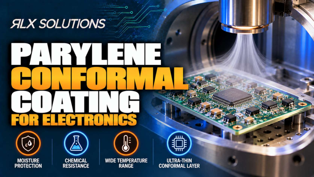
Parylene conformal coating forms a thin protective polymer film over electronic assemblies through a vapour-deposition process, rather than by spraying or brushing liquid material. That difference affects coverage, masking, rework and process planning. RLX Solutions, a contract electronics manufacturer in Concord, Ontario, supports parylene coating as part of electronic assembly programs where the coating specification calls for it.
Parylene is a conformal coating, meaning the deposited film follows the geometry of the printed circuit board, component bodies, leads and exposed surfaces. Unlike liquid coatings, the material reaches the assembly as a vapour. This allows it to coat geometries that are difficult to reach consistently with a directional spray.
That coverage advantage also changes the engineering problem. With parylene, the question is rarely just whether a circuit board should be coated. You need to decide exactly which surfaces may receive coating, which interfaces must remain clean, and how the assembly will be inspected, tested and serviced afterward. For the full picture, see our PCB Assembly Guide.
Parylene coating starts with the assembly, not the coating chamber
A successful parylene process begins before deposition. The manufacturer needs to understand the finished assembly, its keep-out areas and the electrical or mechanical interfaces that cannot tolerate polymer coverage.
Connectors are an obvious example. A connector housing may tolerate coating while its mating contacts cannot. Test points may need electrical access after coating. Grounding surfaces, switches, adjustment points and other functional interfaces can create similar masking requirements.
That makes the assembly drawing part of the coating process. A vague note such as “parylene coat complete board” can leave manufacturing to interpret surfaces that should have been explicitly controlled by the design authority.
A more useful coating package identifies:
- the surfaces intended for coating;
- areas that must remain uncoated;
- connectors and contact surfaces requiring protection;
- test or programming access that must remain usable;
- components or mechanical interfaces with special restrictions; and
- the required inspection or functional test after coating.
The consequence of missing one of these conditions may appear well after deposition. A perfectly coated connector contact is still a manufacturing defect if the coating prevents the connector from functioning.
Worked example: a masked connector changes the process
Consider a hypothetical 6-layer, 1.6 mm printed circuit board measuring 100 × 75 mm. It contains a 0.5 mm pitch board-to-board connector along one edge, two programming headers and six exposed test pads used during functional test.
If the entire assembly enters deposition without defined keep-outs, coating can reach surfaces that need electrical contact later. The coating specification therefore needs to distinguish the protected electronics from the mating connector contacts, programming interfaces and any test pads required downstream.
The board dimensions and layer count do not make that masking decision. The finished assembly architecture does.
Vapour deposition is the defining difference
Liquid conformal coatings begin as material that must be transferred onto the circuit board. Parylene is deposited from the vapour phase, so coverage is less dependent on a spray direction, brush path or the ability of liquid material to flow around a component.
That mechanism matters on densely populated assemblies.
Imagine a tall component positioned close to a smaller package. A directional coating process can create a shadowed region behind the tall component. Vapour can move through small spaces and around three-dimensional features before depositing on exposed surfaces.
The result is useful for assemblies containing closely spaced components, leads and irregular geometry. It does not eliminate process controls. It changes which controls matter most.
Masking becomes particularly significant because vapour can reach places a liquid spray might miss. If an exposed surface is accessible to the deposition environment, engineers should not assume its orientation will protect it.
This is one reason parylene specifications should be written around functional interfaces rather than visual assumptions about which areas appear difficult to coat.
Board A and Board B show why coating cost is not a board-size calculation
Two circuit boards can have identical dimensions and layer counts while requiring substantially different coating preparation.
Consider these hypothetical 8-layer assemblies:
| Decision factor | Board A | Board B |
|---|---|---|
| Layer count | 8 layers | 8 layers |
| Board size | 120 × 80 mm | 120 × 80 mm |
| Thickness | 1.6 mm | 1.6 mm |
| Component density | Moderate | High |
| BGA | One 0.8 mm pitch BGA | Two 0.5 mm pitch BGAs |
| External connectors | One | Four |
| Exposed test points | 4 | 18 |
| Programming interface | Covered after final test | Must remain accessible |
| Masking demand | Limited | Extensive |
| Post-coating access | Minimal | Multiple functional interfaces |
Board B does not become harder to coat because it has eight layers. Its difficulty comes from the finished assembly.
Four connectors create more surfaces that may require selective exclusion. Eighteen test points create more decisions about whether electrical access is needed after deposition. A programming interface that remains in service after coating must be treated differently from one used only before the protective process.
That is why a coating quote based only on board length, width and quantity can miss the manufacturing work. Masking, handling, inspection and downstream testing can distinguish two otherwise similar assemblies.
Masking errors can defeat an otherwise successful coating process
Parylene’s ability to reach exposed geometry makes deliberate masking especially important.
A coating drawing should separate surfaces by function. Electrical contacts are one category. Mechanical mating surfaces are another. Test and programming access may form a third.
This distinction prevents two opposite failures.
The first is unwanted deposition. Coating reaches a surface that must conduct electricity, mate mechanically or remain accessible.
The second is excessive exclusion. Manufacturing masks a much larger area than necessary, leaving electronics exposed simply because the coating requirement was not defined precisely enough.
Use geometry instead of ambiguous notes
Suppose a hypothetical 4-layer circuit board contains a 20-pin connector and the drawing says only “mask J3.”
Does that mean mask the contact area, the complete connector body, the solder joints, or a rectangular region surrounding the component?
Those interpretations produce different coated assemblies.
A better drawing defines the functional boundary. For example, the connector’s mating interface could remain free of coating while surrounding board surfaces receive protection. The manufacturer can then develop the masking operation around an engineering requirement rather than an interpretation.
This is also where design for manufacturability (DFM) becomes relevant. A coating requirement should be reviewed with the actual assembly geometry because component placement can make an apparently simple mask boundary difficult to execute repeatably.
Component placement affects coating manufacturability
Conformal coating is applied after components have already created a three-dimensional surface. Layout decisions therefore influence the coating process even though coating occurs downstream from PCB fabrication and component placement.
Clearance around connectors and other keep-out features can affect masking access. Component orientation can affect how easily masking materials are installed and removed. Closely packed mechanical interfaces can make a simple rectangular exclusion impossible.
For the PCB designer, this creates a useful rule: if a surface must remain electrically or mechanically clean after coating, treat access to that surface as a manufacturing constraint during layout.
That is particularly relevant when the assembly also contains fine-pitch components. The assembly process may already require solder paste inspection (SPI), automated optical inspection (AOI) and X-ray inspection around packages whose solder joints cannot be judged from the outside. Coating should not be treated as an isolated operation that erases the need for those earlier controls.
The manufacturing sequence has to preserve evidence that the assembly was correct before a protective polymer made physical access more difficult.
Inspect and test before coating restricts access
Parylene protects an assembly, but the deposited film can make later troubleshooting and physical access less convenient. Inspection and test strategy should therefore be connected to the coating sequence.
For a new build, first article inspection (FAI) is especially important because it establishes whether the assembly matches the approved manufacturing requirements before the production lot is released. Post-reflow inspection can include AOI, while BGA, land grid array (LGA) and quad flat no-lead (QFN) packages can require X-ray because critical solder joints are hidden underneath the component.
Electrical testing adds another layer of evidence. Flying-probe in-circuit testing (ICT) can provide net coverage for prototype and low-volume builds without a dedicated fixture. Production programs may use bed-of-nails ICT. Functional testing can then exercise the assembly against the customer’s specified pass/fail criteria.
The sequencing question is straightforward: identify defects while the board is still accessible whenever the manufacturing flow allows it.
Worked example: test access determines the coating sequence
Take a hypothetical 10-layer, 1.8 mm board with a 0.5 mm pitch BGA, a QFN power device and 12 functional test pads. The product requires firmware programming through a dedicated header.
One manufacturing flow could complete assembly, SPI, post-reflow inspection, X-ray of hidden joints, programming and functional testing before the final coating operation. If the 12 test pads are no longer needed afterward, the coating requirement can treat them differently from a field-accessible connector.
If firmware updates must still be possible after coating, however, the programming interface becomes a permanent keep-out requirement.
The electrical design did not change. The product’s service strategy changed the coating specification.
Via-in-pad and dense packages make upstream inspection more important
Parylene coating can be specified on assemblies containing dense package structures, but coating does not correct fabrication or soldering defects beneath those packages.
A via-in-pad structure illustrates the point. Plated-over filled via (POFV) construction uses resin fill, copper capping and planarization to create a usable pad surface. That fabrication sequence occurs before component assembly and before conformal coating.
If the board also contains a fine-pitch BGA, the assembly process must establish solder-joint quality before coating. X-ray inspection can examine hidden BGA, LGA and QFN regions where external visual inspection cannot see the complete joint.
The same cause-and-effect relationship applies to underfill. Underfill and conformal coating are different protective processes with different physical roles. If both appear in a manufacturing specification, their interaction and sequence need to be defined rather than assuming one is a substitute for the other.
Potting and encapsulation create another adjacent decision. They surround or cover electronics differently from a thin conformal film, so engineers should choose the protection method based on the mechanical and environmental requirement rather than treating all three processes as interchangeable.
Parylene versus acrylic, silicone and polyurethane is a process decision
Parylene is one of several conformal coating options used for electronic assemblies. Acrylic, silicone and polyurethane coatings are also available, and the important distinction for manufacturing is not simply the polymer name.
The deposition method changes coverage behaviour, masking requirements and the downstream service strategy.
| Engineering consideration | Parylene | Liquid conformal coatings |
|---|---|---|
| Material delivery | Vapour deposition | Liquid application |
| Coverage mechanism | Deposition on exposed surfaces | Spray, dispense or other liquid application |
| Directional shadowing | Reduced dependence on spray direction | Application geometry can matter more |
| Masking importance | High because vapour can reach accessible surfaces | Also required around protected interfaces |
| Rework planning | Should be considered before coating | Depends on coating material and process |
| Drawing quality | Functional keep-outs should be explicit | Selective coating boundaries also need definition |
The decision should begin with the product requirement and the assembly architecture. A board with numerous permanent electrical interfaces presents a different manufacturing problem from a sealed electronic module that will rarely be accessed after final test.
Cost follows that process architecture. A material that provides the desired protection can still be a poor manufacturing choice if the product requires frequent access to coated areas throughout its service life.
Rework belongs in the coating decision before production starts
Conformal coating changes physical access to the assembly. Engineers should therefore consider rework and repair while defining the original manufacturing process, not after a failed board returns from test.
Suppose a 6-layer assembly contains a replaceable QFN device beside a connector that must remain uncoated. If the QFN is coated and later requires replacement, the repair sequence now includes gaining controlled access to the component before removal and restoring the required protective condition afterward.
That adds operations that would not exist on an uncoated assembly.
BGA rework creates an even clearer example because removal, reballing or replacement must ultimately produce a soldered component whose hidden joints can be verified by X-ray. Coating does not replace that verification.
For procurement teams, this matters when evaluating manufacturing cost. The initial coating operation is only one part of lifecycle cost. Serviceability, repair policy, test coverage and the disposition of failed assemblies can all affect whether a coating strategy fits the program.
Treat conformal coating as part of the complete assembly flow
The most reliable coating specification connects fabrication, assembly, inspection, testing and protection instead of placing “parylene coat” as an isolated note near the end of a drawing.
- Fabricate the bare board. Stackup, via architecture, surface finish and pad geometry must support the component design.
- Assemble components. Solder paste deposition, placement and reflow establish the electrical assembly.
- Inspect hidden and visible joints. SPI, AOI, X-ray and manual inspection are applied as required by the assembly.
- Program and electrically test. Programming, ICT or functional testing should occur where the manufacturing plan requires electrical access.
- Prepare the assembly for coating. Keep-outs and protected interfaces are identified and masked.
- Apply the specified coating. The deposition process covers the surfaces defined by the manufacturing documentation.
- Complete required post-process verification. The finished assembly must still satisfy the customer’s inspection and functional requirements.
Changing one stage can affect the stages after it. Moving programming from step four to a post-coating operation, for example, means the programming interface must remain accessible. Adding a connector late in the design can create another masking boundary. Moving test entirely downstream can require previously disposable test access to remain free of coating.
This is why conformal coating belongs in design for assembly (DFA) discussions rather than appearing for the first time when production documentation is released.
What the manufacturer needs before quoting a coated assembly
A coating requirement becomes easier to execute when the manufacturer receives the complete assembly definition rather than a coating name in isolation.
For a PCB assembly, the manufacturing package can include the bill of materials (BOM), pick-and-place or centroid data, assembly drawing and the underlying board manufacturing files. Gerber RS-274X, ODB++, IPC-2581 and NC drill files are accepted manufacturing formats, while stackup information, impedance targets and fabrication notes provide additional board context.
For the coating operation itself, the assembly drawing should communicate where coating belongs and where it cannot go.
That information gives the engineer-reviewed DFM process something concrete to evaluate. The review can then consider whether component placement, connectors, test access, programming access and other interfaces create manufacturing conflicts before the build reaches coating.
Procurement should also keep coating requirements synchronized with revisions. If a connector moves or a new test point appears but the coating drawing remains at the previous revision, the manufacturing package contains two different definitions of the finished product.
Make the coating requirement part of the quote package
If you are specifying parylene on a circuit board heading into production, RLX reviews the assembly as part of every quote. Send the Gerbers or other accepted manufacturing data, BOM, pick-and-place file and assembly documentation so coating, inspection, testing and relevant keep-outs can be considered together rather than as disconnected operations.
Frequently Asked Questions
What is parylene conformal coating used for on electronics?
Parylene is a conformal coating applied to electronic assemblies using vapour deposition. The deposited polymer follows exposed board and component geometry, including areas that may be difficult to reach with a directional liquid application. Its suitability should be considered together with masking, electrical interfaces, test access and the assembly’s expected service or rework requirements.
Can parylene coating be applied to a fully assembled PCB?
Yes, parylene is a conformal coating process for assembled electronics. Before coating, the manufacturing plan needs to identify surfaces that must remain accessible or free of deposition. Connectors, electrical contacts, programming interfaces and test points are common examples. Inspection and electrical testing should also be planned around the point at which coating changes physical access to the assembly.
Should a PCB be functionally tested before parylene coating?
Testing before coating can identify assembly defects while components and electrical access points remain readily accessible. The exact sequence follows the customer’s manufacturing and test requirements. Available assembly test methods include flying-probe ICT, bed-of-nails ICT and functional testing to a customer specification, with pass/fail logging and serial traceability available for functional test.
Can BGA assemblies receive conformal coating?
A ball grid array (BGA) can be part of a conformally coated electronic assembly, but hidden solder-joint quality should be addressed through the assembly inspection process. X-ray inspection is available for BGA, LGA and QFN packages, including void analysis. Coating is a protective process and does not replace verification of the solder joints beneath the package.
Is parylene the only conformal coating option for electronic assemblies?
No. Available conformal coating processes include acrylic, silicone, polyurethane and parylene, with selective or full-board application available. The appropriate specification depends on the product’s protection requirement, assembly geometry, keep-outs, testing sequence and service strategy. Engineers should define the functional requirement and coating boundaries before manufacturing rather than selecting a coating solely by material name.
What files should I provide for a conformally coated PCB assembly quote?
Provide the manufacturing and assembly data needed to define the complete build. Accepted PCB manufacturing formats include Gerber RS-274X, ODB++, IPC-2581 and NC drill. PCB assembly documentation includes the BOM, pick-and-place or centroid file and assembly drawing. Add clear coating instructions and keep-outs so the protective process can be reviewed with the actual assembly geometry.