
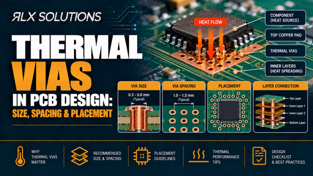
Thermal Vias in PCB Design: Size, Spacing & Placement
Thermal vias conduct heat through a printed circuit board by using plated hole walls to connect copper between layers. RLX
Thermal vias conduct heat through a printed circuit board by using plated hole walls to connect copper between layers. RLX

High-speed PCB design works when stackup, routing geometry and return paths are engineered as one system rather than three separate
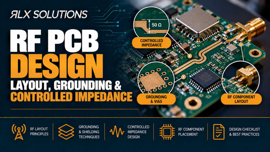
RF PCB design succeeds when the stackup, transmission-line geometry, return path and fabrication process are treated as one electrical system.

A PCB design review before production should confirm the stackup, drill plan, copper geometry, impedance targets, component data, assembly clearances,
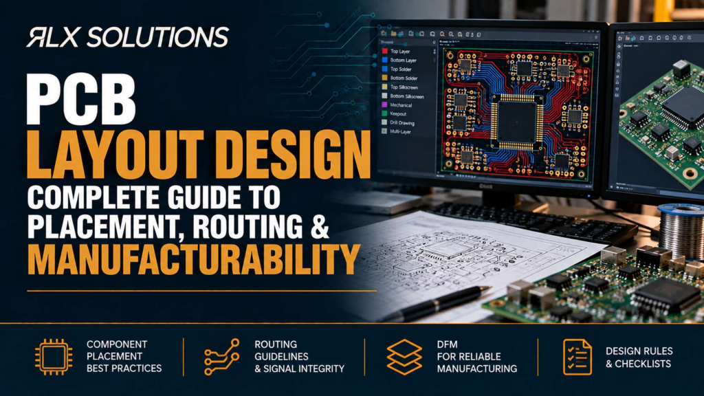
PCB layout design turns a schematic into a physical circuit board by assigning component locations, copper geometry, layer usage, vias,
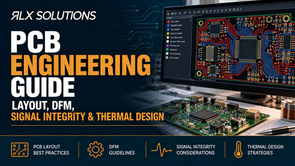
PCB engineering turns schematic intent into a printed circuit board that can be fabricated, assembled, tested and operated without electrical