

Power Integrity in PCB Design: How to Build a Stable Power Delivery Network
Power integrity in PCB design means keeping voltage at each load within its operating limits as current changes across frequency.
Power integrity in PCB design means keeping voltage at each load within its operating limits as current changes across frequency.
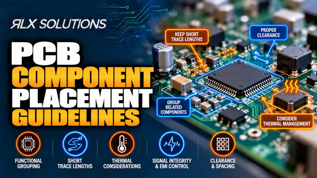
PCB component placement should support electrical performance, soldering, inspection, testing and rework at the same time. RLX Solutions, a contract
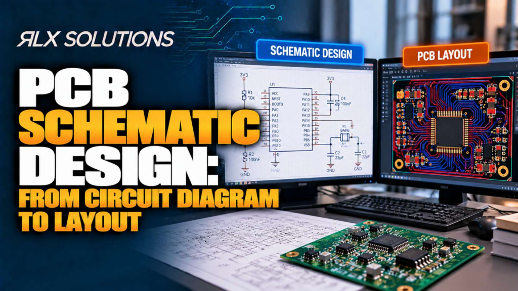
PCB schematic design turns an electrical circuit into the data needed for a manufacturable printed circuit board. The schematic defines

Design for manufacturability (DFM) asks whether your printed circuit board can be fabricated reliably. Design for assembly (DFA) asks whether

Differential pair routing works when impedance, coupling, reference geometry and electrical length are treated as one system rather than separate
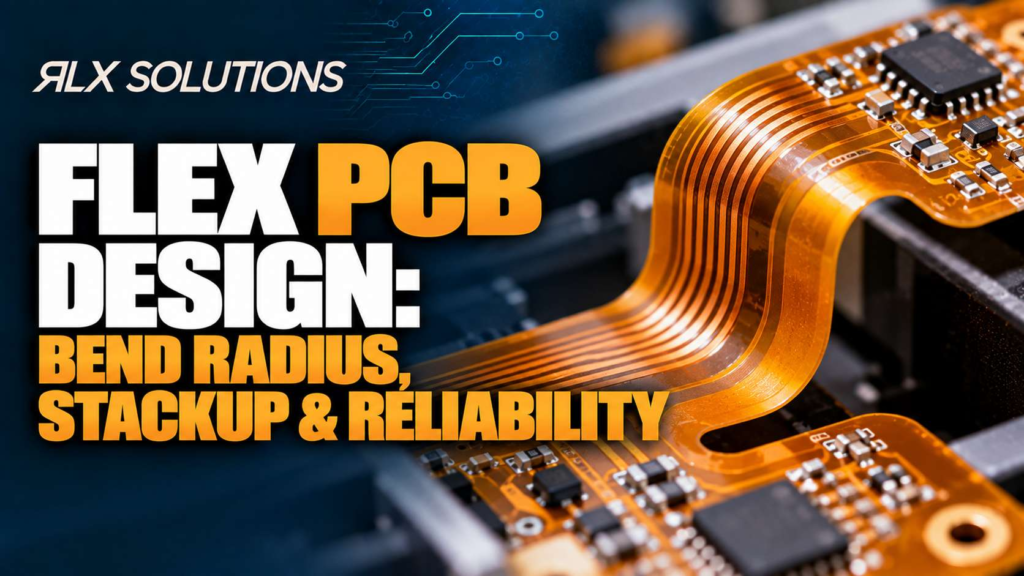
Flex PCB design succeeds when bend radius, copper geometry and stackup are treated as one mechanical system rather than separate

Creepage is the shortest path between conductors along an insulating surface, while clearance is the shortest distance through air. PCB

PCB ground plane design is primarily a return-path problem: keep the reference plane continuous, keep return current close to its

High-voltage PCB design requires separate control of clearance through air, creepage across insulating surfaces and isolation through solid dielectric. The
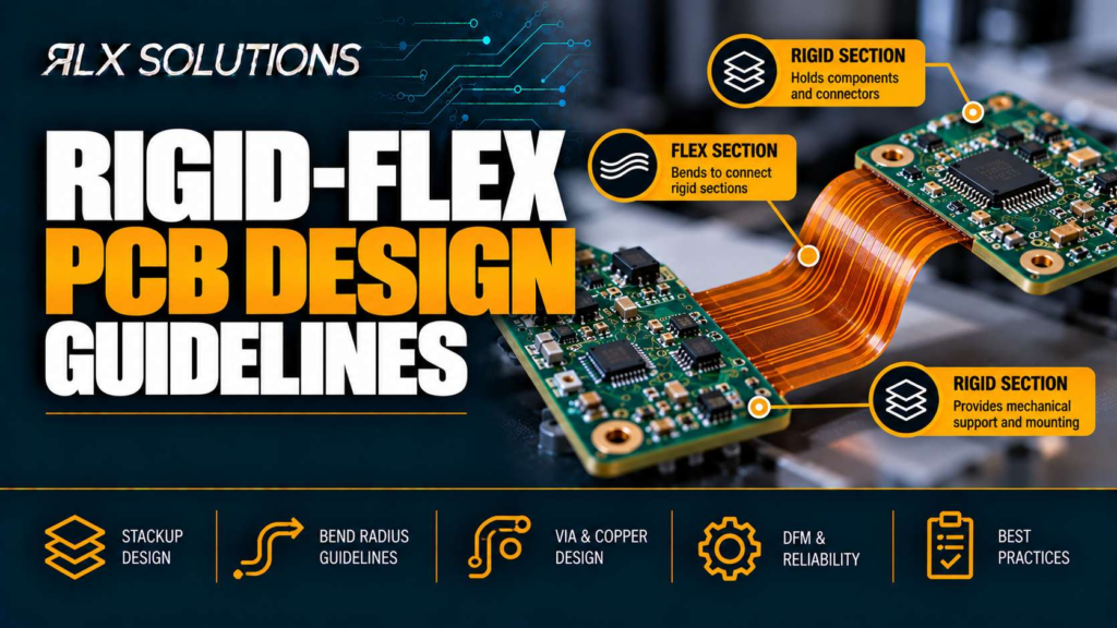
Rigid-flex PCB design guidelines start with one rule: treat the flex region as a mechanical structure, not simply another PCB