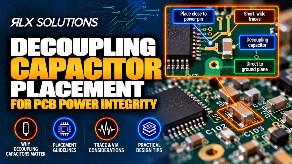
Decoupling capacitor placement is a power integrity problem, not a distance-to-pin rule.
The capacitor must provide a low-impedance current path at the frequencies where the load
switches, which makes loop geometry, planes, vias and package inductance as important as
physical proximity. RLX Solutions, a contract electronics manufacturer in Concord, Ontario,
reviews these relationships during PCB design and layout work.
Place the Capacitor to Minimise the Complete Current Loop
A decoupling capacitor stores local charge and supplies transient current when an integrated
circuit changes state faster than the upstream power system can respond. Its effectiveness
depends on the impedance of the complete path from the capacitor to the load and back.
That path includes:
- capacitor equivalent series resistance and inductance
- pad and escape geometry
- power and ground vias
- power and ground planes
- package connections between PCB pads and the die
This is why a capacitor 2 mm from an IC pin can perform worse than one 4 mm away. If the
2 mm placement requires long pad traces and widely separated vias, while the 4 mm placement
connects almost directly into tightly coupled power and ground planes, the nominally farther
capacitor can present the lower-inductance path.
At high frequency, trace length alone is therefore an incomplete placement metric. Loop area
and connection geometry tell you more about whether the capacitor can supply a fast transient.
Follow the transient current path
Consider a hypothetical 1.0 V rail feeding a processor. A 100 nF capacitor sits beside the
device. During a fast load transition, current should flow from the capacitor’s power terminal
into the device, through the switching circuitry, out through ground and back to the
capacitor’s ground terminal.
Every section of that loop contributes inductance. Moving the capacitor closer shortens one
part of the path. Moving its power and ground vias closer to the capacitor pads can shorten
another. Connecting both terminals into adjacent power and ground planes can reduce the
effective loop area further.
This is the mechanism behind good placement. You are not positioning a component near a pin
for its own sake. You are engineering the transient-current loop between the capacitor, the
printed circuit board and the load.
Via Placement Can Matter as Much as Capacitor Placement
Once power and ground are carried on internal planes, the vias beside the capacitor become
part of the decoupling network. A short component-to-via connection keeps the surface portion
of the current path from consuming the electrical advantage created by a nearby capacitor.
Worked example: a six-layer power connection
Consider a hypothetical six-layer, 1.6 mm circuit board with the following stackup:
- Layer 1: components and signals
- Layer 2: ground
- Layer 3: 1.0 V power
- Layer 4: signals
- Layer 5: ground
- Layer 6: signals
A 0402 decoupling capacitor on Layer 1 connects to Layer 3 power and Layer 2 ground. If short
traces run outward from both capacitor pads before reaching their vias, those traces become
part of the high-frequency current path. Moving the vias immediately beside the pads removes
unnecessary surface routing and allows the closely spaced Layer 2 and Layer 3 planes to carry
more of the path.
The same reasoning applies at the IC connection. A well-placed capacitor cannot indefinitely
compensate for an inductive package escape or an unnecessarily long IC-to-plane path. Power
integrity therefore has to be considered from the capacitor terminals through the PCB and
into the package, rather than stopping at the component courtyard.
Avoid adding inductance after choosing the capacitor
Capacitor selection and PCB layout cannot be separated. A small multilayer ceramic capacitor
may have useful high-frequency electrical characteristics, but its mounted behaviour also
includes the pads, traces and vias used to connect it.
Connection inductance can shift the frequency range over which the installed capacitor is
effective. That becomes increasingly relevant as edge rates rise. The power delivery network
(PDN), meaning the complete electrical path that delivers power from the source to the load,
must maintain acceptable impedance across the frequencies that matter to the load transient.
Board A vs Board B: Same Layer Count, Different Power Integrity
Two boards can use the same layer count, capacitor values and bill of materials yet behave
differently because the physical connections change the mounted impedance. The fabrication
drawing alone will not reveal that difference unless the stackup and interconnect geometry
are examined together.
Consider two hypothetical eight-layer boards, each 1.6 mm thick. Both use a 0.8 mm pitch BGA
and place a 100 nF capacitor 3 mm from the package edge.
| Decision Factor | Board A | Board B |
|---|---|---|
| Layer count | 8 | 8 |
| Board thickness | 1.6 mm | 1.6 mm |
| BGA pitch | 0.8 mm | 0.8 mm |
| Capacitor distance from package | 3 mm | 3 mm |
| Capacitor connection | Surface traces before vias | Vias immediately beside pads |
| Power and ground via geometry | Vias separated by routing | Vias kept close to capacitor terminals |
| High-frequency consequence | Larger connection loop | Smaller connection loop |
| Manufacturing consequence | Simpler local routing | Placement and drilling geometry require tighter coordination |
Board A demonstrates why a placement rule expressed only in millimetres is incomplete.
Its capacitor is close to the package, but current still travels through extra surface
conductor before entering the planes. Board B uses the same nominal capacitor distance but
reduces the connection loop by placing the plane transitions close to the capacitor pads.
The cost difference may emerge indirectly. If Board B can achieve the required PDN behaviour
with conventional through vias, its fabrication architecture can remain relatively simple.
If density around the BGA forces the design toward blind vias, microvias or via-in-pad
structures, the manufacturing sequence changes. The electrical decision and fabrication
decision have become the same design problem.
Use the Stackup to Make Decoupling Placement Work
Capacitor placement cannot repair a stackup that creates a poor power-return geometry. Power
and ground planes with useful coupling provide a distributed path that complements discrete
decoupling capacitors. Their position in the stackup therefore influences how the current
reaches the capacitor and the IC.
A power plane buried deep in the board can require a longer vertical transition than a plane
close to the component surface. The practical question is not simply which layer carries the
rail. It is how the chosen power layer, its reference plane, the capacitor and the load form
the complete current path.
Plane changes can move the placement problem into the Z-axis
Suppose a 12-layer board has a high-current processor on Layer 1. One design places its main
ground plane on Layer 2 and a local power plane on Layer 3. Another assigns the same power rail
to Layer 10. A capacitor can occupy the same X-Y coordinates in both layouts while seeing a
very different vertical interconnect.
The second arrangement requires the designer to examine the longer via path and the planes
crossed on the way to the rail. Moving a capacitor 1 mm closer to the package may have less
effect than changing how that capacitor reaches its power and return structures.
Stackup planning should therefore happen before dense component placement is frozen. If the
PDN architecture is decided after BGA breakout, signal routing and mechanical constraints have
consumed the available space, the engineer may be forced into more complicated via structures
simply to recover an acceptable connection.
Dense BGA Escape Changes the Decoupling Strategy
Fine-pitch packages create a physical competition between signal escape, power delivery,
decoupling and manufacturability. As pitch decreases, the available routing channels around
the package shrink, and conventional through vias can consume locations that would otherwise
be used for capacitor connections or signal breakout.
Via-in-pad plated over (POFV) places a via within a component pad, then uses resin fill,
copper capping and planarisation to restore a solderable surface. Electrically, this can
shorten the path from a BGA pad into an internal plane. Manufacturing-wise, it adds processes
that must be designed into the fabrication package rather than treated as an ordinary drilled
via.
Blind vias connect an outer layer to one or more internal layers without passing through the
complete PCB. On multilayer builds they change the lamination and drilling sequence.
Microvias use laser drilling for small interlayer connections and can be arranged in stacked
or staggered structures when density demands it.
Worked example: conventional escape versus microvia escape
Consider a hypothetical 10-layer board carrying a dense BGA. Board A uses through vias for
breakout and places decoupling capacitors around the package perimeter. Board B uses Layer 1
to Layer 2 microvias beneath selected pads, with additional Layer 2 to Layer 3 connections
where the architecture requires them.
Board B may give the layout engineer more direct access to internal power and ground
structures, but it also introduces laser-drilled connections and a more involved fabrication
sequence. If via-in-pad is used, filling, capping and planarisation also become part of the
build.
The engineering decision is therefore not “microvias are better for decoupling.” The question
is whether the density and PDN target justify changing the via architecture. If conventional
geometry can produce the required current path without blocking signal escape, adding HDI
structures solely to make the capacitor appear closer can increase manufacturing burden
without solving a demonstrated electrical problem.
Do Not Treat Every Decoupling Capacitor as Electrically Equivalent
A bank of capacitors is intended to shape PDN impedance across a frequency range. The
capacitor closest to a particular power pin may serve a different part of that range from
larger bulk capacitance elsewhere on the circuit board.
Bulk capacitance supports slower changes in current demand. Smaller local capacitors are
generally used where faster transient response is required. The voltage regulator module,
planes, discrete capacitors, vias, package and die capacitance all participate in the
resulting network.
That network can exhibit resonances. Adding more nominal capacitance does not automatically
guarantee lower impedance at every frequency because each physical capacitor has parasitic
resistance and inductance and interacts with the rest of the PDN.
This is why placement should follow the electrical objective for each group of capacitors.
The highest-frequency local components usually deserve the most attention to connection
inductance. Larger energy-storage capacitors can often tolerate a longer electrical path
because they are addressing a different portion of the transient response.
Placement Errors Often Surface as System-Level Failures
A weak decoupling layout does not necessarily announce itself as a “capacitor placement”
fault. The symptom may appear as rail droop, timing instability, unexpected resets, data
errors or electromagnetic interference. That makes the root cause harder to isolate after
fabrication.
Consider a processor rail that behaves normally during low activity but becomes unstable when
several internal blocks switch simultaneously. Replacing the regulator may not address the
problem if the regulator is separated from the load by enough interconnect inductance that it
cannot supply the fastest part of the transient. Local capacitance and its connection path
then become central to the investigation.
The schedule consequence is significant. Moving a capacitor before layout release may take
minutes. Discovering the same problem during prototype validation can require measurement,
rework, another layout revision and another bare-board build. Placement review therefore has
value even when it does not alter the schematic.
Give the Manufacturer Enough Information to Preserve the PDN
Power integrity intent can be lost when the fabrication package describes geometry without
communicating the stackup and controlled electrical requirements behind it. The manufacturer
needs enough information to determine whether the proposed layer construction and via
architecture can be built as intended.
For a board where decoupling performance depends heavily on the stackup, prepare:
- Gerber RS-274X, ODB++ or IPC-2581 fabrication data
- NC drill data identifying the required holes
- a stackup drawing showing layer functions
- impedance targets where controlled impedance is required
- fabrication notes identifying special via structures
- assembly drawings showing component orientation and placement intent
- a bill of materials and pick-and-place data for assembly
The objective is to prevent an electrically meaningful structure from becoming an accidental
manufacturing assumption. A via that exists specifically to minimise a decoupling loop should
not be treated as interchangeable with a connection whose location is mechanically
convenient.
This is also where design for manufacturability (DFM) intersects with power integrity.
Aspect ratio, drilled-hole geometry, annular rings, via filling and sequential lamination can
determine whether the electrical architecture can be fabricated consistently. Changing any
of those features after routing is complete can force the layout back into placement and
escape decisions that should have been resolved earlier.
Review Placement Before the Layout Becomes Expensive to Change
The best point to review decoupling placement is after the stackup, package escape strategy
and major power domains are understood, but before routing has made those decisions difficult
to move. At that stage, the engineer can still change layer assignments, via locations and
capacitor orientation without unravelling large sections of the board.
Review each important rail by tracing the current path rather than counting capacitors.
Identify where the capacitor enters the power structure, where its return enters ground and
how the load connects to the same structures. Then examine whether routing, via separation or
layer transitions introduce avoidable inductance.
For dense boards, extend the review into fabrication. If a 0.3 mm pitch BGA, via-in-pad,
blind vias or laser-drilled microvias are part of the architecture, their manufacturing
requirements need to be resolved alongside the electrical layout. An electrically attractive
geometry is useful only if the complete stackup can support it.
Turn Power Integrity Intent into Manufacturable Geometry
If you are preparing a printed circuit board where decoupling placement, stackup or BGA escape
affects the PDN, RLX can review the design as part of the quote process. Send the fabrication
files, stackup information and, for assembly, the BOM and pick-and-place data so electrical
intent can be considered alongside engineer-reviewed DFM before production release.
Frequently Asked Questions
How close should a decoupling capacitor be to an IC?
There is no universal distance that guarantees good decoupling. Place the capacitor so the
complete current loop through its pads, vias, planes and IC connection has low inductance.
A slightly farther capacitor with direct plane connections can be electrically preferable to
a closer capacitor connected through longer surface traces or poorly positioned vias.
Should the decoupling capacitor connect to the pin before the power plane?
Treat this as a current-path problem rather than applying a fixed routing sequence. For a
device connected through internal power and ground planes, capacitor and IC via geometry may
dominate the high-frequency path. Trace the physical loop through the actual stackup and
minimise unnecessary conductor length and loop area instead of relying on a schematic-style
pin-to-capacitor-to-plane rule.
Can I put decoupling capacitors on the opposite side of the PCB?
Yes, if the resulting electrical path meets the PDN requirement. Opposite-side placement adds
vertical interconnect and makes via geometry important, but it can be useful beneath a BGA or
another dense package where top-side space is limited. Evaluate the capacitor, vias, planes
and package connection as one network rather than judging placement from X-Y distance alone.
Does via-in-pad improve decoupling capacitor performance?
Via-in-pad can shorten connections where package density makes conventional routing
difficult, but it changes fabrication. A plated-over structure requires filling, copper
capping and planarisation to create a suitable pad surface. Use it when the electrical and
density requirements justify the architecture, rather than as a default replacement for
conventional capacitor and via placement.
Do more decoupling capacitors always improve power integrity?
No. The installed PDN includes capacitor parasitics, connection inductance, planes, vias,
package behaviour and the power source. These elements interact across frequency, so adding
capacitance without considering the resulting impedance can miss the actual problem. Start
from the rail’s transient requirements and evaluate which capacitor locations and values
address the required frequency range.
What files help with a PCB power integrity and DFM review?
Provide the fabrication data, NC drill files, stackup documentation and impedance targets
where applicable. For assembly, include the bill of materials, pick-and-place data and
assembly drawing. Clearly identify special via structures and other fabrication requirements
so the physical build can be reviewed against the electrical layout before release.