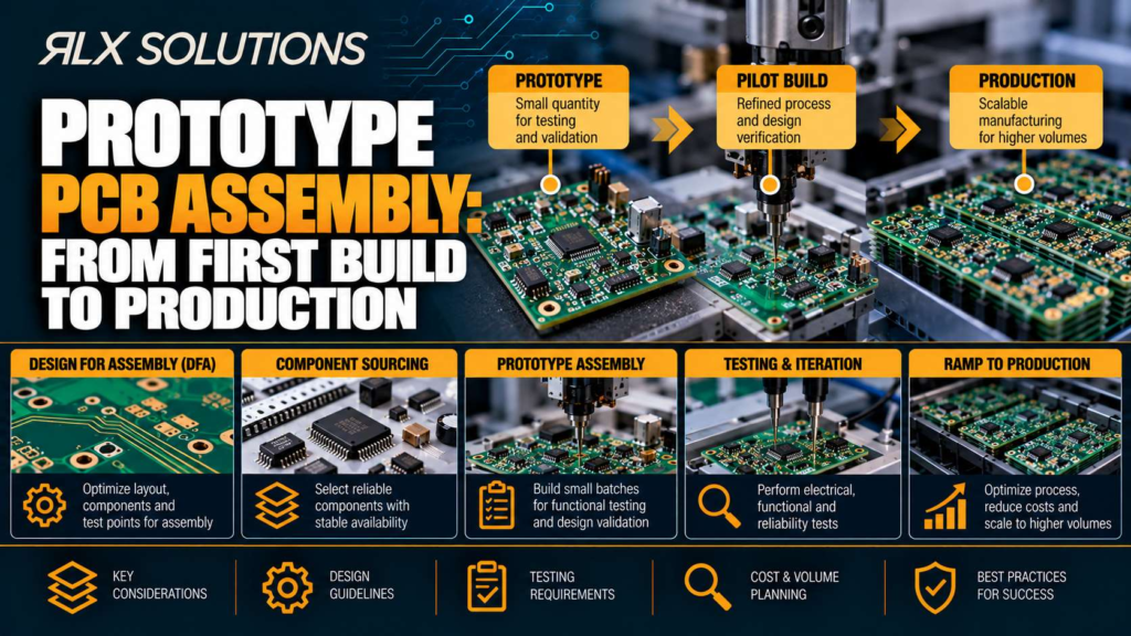
Prototype PCB assembly should prove that a circuit board can be built, inspected, tested and repeated, not simply that one assembled unit powers on. RLX Solutions, a contract electronics manufacturer in Concord, Ontario, uses the first build to expose design, sourcing and process issues before they become production problems.
A Prototype PCB Assembly Should Prove the Manufacturing Process
A working prototype answers an important question: does the design function? It does not automatically answer the next question: can the same design be manufactured repeatedly at production volume? For the full picture, see our PCB Assembly Guide.
That distinction changes what you should expect from prototype assembly.
A useful first build generates evidence about solder paste deposition, component placement, reflow results, hidden joints, through-hole operations, component sourcing and test coverage. It also exposes mismatches between the bill of materials (BOM), centroid data, assembly drawing and the physical printed circuit board.
The goal is process learning without creating a prototype-only process that must be reinvented later.
Consider a hypothetical 6-layer, 1.6 mm board with a 0.5 mm pitch ball grid array (BGA), 0402 passives and several through-hole connectors. Building five units by hand might demonstrate electrical function. It would reveal much less about repeatability than running the surface-mount devices through the intended stencil, placement and reflow sequence, then completing the through-hole operation under controlled workmanship criteria.
That difference matters when the next order is 250 boards rather than five.
Start With Manufacturing Data That Describes One Revision
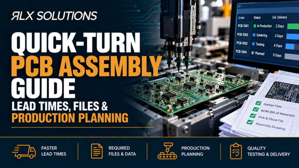
Assembly problems often begin before the first component reaches the line. The fabrication data, BOM, pick-and-place file and drawings must describe the same board revision.
For prototype PCB assembly, the manufacturing package should normally contain:
- Bare-board manufacturing data: Gerber RS-274X, ODB++, or IPC-2581 data with NC drill information.
- BOM: An .xlsx or .csv file identifying the components required for the assembly.
- Pick-and-place data: Centroid information that defines component locations and rotations.
- Assembly drawing: The visual manufacturing reference for component placement and assembly requirements.
- Fabrication information: Stackup, impedance targets and fabrication notes where the design requires them.
A mismatch between these files creates ambiguity at exactly the point where you want the prototype to establish a controlled process.
Take a 10-layer board where the BOM has advanced to Revision C but the pick-and-place file still represents Revision B. If C37 moved 2 mm during the layout revision, the BOM alone cannot tell the placement process that its coordinates changed. The problem is document control, not placement accuracy.
An engineer-reviewed design for manufacturability (DFM) and design for assembly (DFA) review should therefore happen before build release. The most valuable corrections are the ones made before material has been committed and the line has been set up.
Component Sourcing Is Part of Prototype Risk
The prototype sourcing decision affects what the build actually proves.
There are three practical assembly models. In a turnkey build, the manufacturer handles component procurement along with the build. A kitted or partial-turnkey build lets you provide selected parts while the manufacturer sources the balance. A consigned build uses a complete customer-supplied kit.
The distinction becomes important when parts are scarce, expensive, obsolete or sensitive to substitution.
Suppose a prototype uses a microcontroller in a 0.5 mm pitch package and a power regulator whose specified manufacturer part number is temporarily constrained. Substituting the regulator without engineering approval might get hardware onto the bench faster, but it also changes the configuration being validated. Electrical performance, thermal behaviour or surrounding passive values may differ.
Sourcing controls also matter when parts move outside authorized distribution. Counterfeit prevention can involve source vetting, packaging and date-code checks, visual inspection, lot verification, X-ray, electrical testing and, where required, escalation to decapsulation and die analysis.
Moisture-sensitive device handling is another assembly variable rather than an administrative detail. Packaging integrity and controlled storage matter because absorbed moisture can create package damage during reflow.
Prototype procurement should therefore answer two separate questions: can the required parts be obtained, and can their identity and condition be established well enough for the prototype results to mean something?
Bare PCB Decisions Follow the Assembly Into Production
Assembly cannot compensate for a bare board whose construction conflicts with component geometry or electrical requirements.
Via architecture is a common example. A conventional plated through-hole passes through the full board. Blind and buried vias change which layers connect and can introduce additional fabrication stages. Via-in-pad construction can require resin filling, copper capping and planarization so the component pad remains suitable for assembly.
Consider two hypothetical 10-layer boards:
| Decision factor | Board A | Board B |
|---|---|---|
| Layer count | 10 layers | 10 layers |
| Via architecture | Through vias only | Layer 1 to 2 and Layer 2 to 3 microvias plus buried vias |
| Example laser-drilled hole | None | 0.10 mm |
| Assembly package | 0.8 mm pitch BGA | 0.4 mm pitch BGA |
| Fabrication sequence | Conventional multilayer route | Additional HDI build stages |
| Assembly concern | Standard fanout leaves more routing area | Dense escape routing increases dependence on pad and via construction |
These boards have the same layer count, but they are not equivalent manufacturing jobs. Board B creates additional fabrication dependencies before assembly begins.
That is why comparing prototype prices by layer count and board dimensions alone can be misleading. A dense high-density interconnect (HDI) architecture can change drilling, lamination, filling, capping and inspection requirements while the headline layer count stays unchanged.
Aspect ratio deserves the same attention. A hypothetical 2.0 mm thick circuit board with a 0.20 mm finished hole has a 10:1 thickness-to-hole relationship. Reduce that hole diameter while keeping the board thickness constant and plating becomes more demanding. The assembly drawing will not fix a hole architecture that should have been resolved during fabrication engineering.
Paste Printing and Placement Create the First Process Evidence
For surface-mount technology (SMT), solder paste printing determines how much solder reaches each joint before placement and reflow.
Solder paste inspection (SPI) can measure paste volume, area and offset before the board enters reflow. That timing is significant. A paste defect found before reflow is a process condition that can still be investigated before it becomes a solder-joint defect.
Placement then adds another set of variables. Package pitch, component orientation, pad geometry and machine data all have to agree.
A prototype containing 01005 passives and a 0.3 mm pitch BGA, for example, presents a different placement problem from a board dominated by 0603 passives and a 1.0 mm pitch BGA. Both are SMT assemblies, but the smaller geometries reduce the room available for errors in paste registration, placement and pad design.
This is why the prototype should preserve manufacturing observations. If a component repeatedly shifts, bridges or produces insufficient solder, replacing it by hand may produce a working engineering sample while hiding the process condition that needs correction.
Rework can save a prototype. It should not erase the evidence the prototype was meant to produce.
Inspection Must Match the Joint You Are Trying to See
No single inspection method sees every assembly defect.
Automated optical inspection (AOI) is effective after reflow for visible placement and solder conditions on both sides of a board. Manual visual inspection under magnification adds workmanship assessment. Neither can directly inspect every hidden solder interface beneath packages such as BGAs, land grid arrays (LGAs) or quad flat no-lead (QFN) devices.
Automated X-ray inspection (AXI) addresses that visibility problem. It can be used for BGA and LGA joints, QFN thermal pads and void analysis.
The mechanism matters. A solder joint hidden beneath a package can look perfectly acceptable from the board perimeter because the defect is physically outside the optical line of sight. X-ray inspection looks through the assembly instead of trying to infer the hidden joint from its exterior.
A prototype with a large BGA can therefore pass visual inspection while still needing X-ray evidence before you know what happened beneath the package.
IPC-A-610 Class 2 and Class 3 also affect workmanship expectations. Class 3 applies tighter workmanship requirements than Class 2. The assembly class should be established as a manufacturing requirement rather than treated as a label added after inspection.
Electrical Test Should Grow With What You Need to Prove
Inspection asks whether the assembly appears to have been manufactured correctly. Electrical testing asks different questions.
Flying-probe in-circuit test (ICT) is useful for prototype and low-volume work because it can provide net coverage without requiring a dedicated fixture. Bed-of-nails ICT becomes relevant in production where a fixture is justified by the repeated build. Functional test (FCT) verifies operation against a customer-defined test specification and can record pass or fail results with serial traceability.
These methods are complementary.
Imagine a 4-layer controller with 600 populated components, a 0.5 mm pitch processor and two external connectors. A functional test might prove that the board boots, communicates and drives its outputs. It may not isolate every assembly fault efficiently. Electrical net testing can give different diagnostic information.
Now suppose the same design moves from 20 prototype units to 2,000 production units. A fixture that made little economic sense at 20 pieces can become relevant because its engineering cost is distributed across a much larger lot and repeated test cycles.
The important production question is therefore not simply, “Did the prototype pass?” It is, “What test method produced that result, and will that method still make sense at the intended quantity?”
First-Article Approval Creates the Production Baseline
A first article is the point where manufacturing evidence becomes a release decision.
The first-article inspection (FAI) should occur before the production lot is released. That gives the customer a controlled opportunity to review the new build rather than discovering an interpretation difference after the full quantity has been assembled.
This stage is especially important when assembly documentation contains choices that cannot be derived safely from the PCB data alone. Polarity, mechanical hardware, connector orientation, programming requirements, special workmanship instructions and functional test expectations may all require explicit documentation.
The first article also gives engineering changes a clean boundary.
If the prototype exposes a footprint problem and the PCB layout changes before the next build, the revised hardware is not simply “the same prototype with a fix.” It is a new manufacturing revision. The fabrication package, BOM, centroid data and assembly drawing should move together so the approved configuration remains identifiable.
That discipline becomes more valuable as quantities increase because informal knowledge does not scale with the lot.
Prototype and Production Builds Can Share a Design but Carry Different Cost
Unit price is shaped by manufacturing work, not simply board count.
Two assemblies with the same outline and layer count can have very different process demands. Fine-pitch placement, BGA X-ray inspection, mixed SMT and through-hole assembly, programming, conformal coating, underfill, selective soldering and functional testing each introduce work that may remain invisible in a basic PCB description.
The same applies to sourcing.
A board populated entirely from available authorized-distribution stock creates a different procurement problem from one containing an end-of-life integrated circuit that requires lot verification and additional authenticity testing.
This is why prototype cost should be read as information about the manufacturing route, not extrapolated mechanically into production pricing.
The prototype is also where you can remove unnecessary production work. If a layout change eliminates repeated rework, if a test-point change makes electrical testing easier, or if a component choice removes a sourcing problem, the value appears later across every production unit.
Move to Production Without Resetting What the Prototype Taught You
The strongest prototype-to-production transition preserves configuration, process knowledge and test intent.
Before increasing quantity, engineering and procurement should be able to identify:
- the approved PCB revision and matching manufacturing files;
- the released BOM and any approved sourcing decisions;
- the pick-and-place data and assembly drawing for that revision;
- the required workmanship class;
- inspection requirements for hidden and visible joints;
- programming and serialization requirements where applicable;
- electrical and functional test requirements;
- the approved first article and any changes made after it.
This is also the point to reconsider the test architecture. A flying-probe approach suited to prototypes may give way to fixture-based ICT at production volume. Functional test procedures may need clearer pass/fail logging. Serialization can tie those results to individual assemblies.
Special processes need the same discipline. Conformal coating, underfill, potting, in-system programming, press-fit insertion and selective soldering should be treated as controlled manufacturing operations rather than additions that appear after the prototype has already been approved.
A production release is therefore a transfer of a known configuration into a repeatable process. If engineering changes continue after first-article approval, control the revision rather than allowing the production line to inherit prototype-era exceptions.
Prepare the Prototype So the Next Build Can Scale
A prototype PCB assembly has done its job when it leaves you with more than functioning hardware. It should leave you with a buildable revision, resolved manufacturing questions, an inspection path, sourcing decisions and test evidence that can follow the circuit board into production.
If your next build needs to establish that baseline, RLX can review the manufacturing package as part of the quote process. Send the Gerbers or other accepted fabrication data, BOM, pick-and-place file and assembly drawing so the build can be reviewed before release.
Frequently Asked Questions
What files do I need for prototype PCB assembly?
For assembly, prepare the BOM, pick-and-place or centroid data and assembly drawing. The bare-board package can use Gerber RS-274X, ODB++, or IPC-2581 data with NC drill information. Add the stackup, impedance targets and fabrication notes where the design requires them. Keeping every file on the same revision prevents avoidable manufacturing ambiguity.
Can I supply my own components for a prototype build?
Yes. A kitted build can use customer-supplied critical or long-lead parts while the manufacturer sources the remainder. A consigned build uses a complete customer-supplied kit. Turnkey assembly places component procurement with the manufacturer. The best structure depends on which parts you need to control and which sourcing work you want included.
How are BGAs inspected during prototype assembly?
BGA solder joints are hidden beneath the package, so optical inspection alone cannot see the complete interface. X-ray inspection can evaluate BGA joints and is also applicable to LGAs, QFN thermal pads and void analysis. AOI and manual visual inspection remain useful for visible assembly conditions, so the methods address different defect opportunities.
Is flying-probe testing suitable for prototype circuit boards?
Flying-probe ICT is well suited to prototypes and low-volume builds because it does not require a dedicated bed-of-nails fixture and can provide full net coverage. At production quantities, fixture-based ICT may become more appropriate. Functional testing can then verify board behaviour against the customer’s test specification and record pass or fail results.
What happens before a prototype PCB assembly moves into production?
The new build should pass first-article inspection and receive customer approval before the production lot is released. Any resulting design change should be reflected consistently across the fabrication data, BOM, pick-and-place information and drawings. Production also gives you reason to reassess test fixtures, serialization and any special assembly processes required at scale.
Can prototype PCB assembly use IPC-A-610 Class 3 workmanship?
Yes. PCB assembly can be built to IPC-A-610 Class 2 or Class 3 workmanship requirements. Class 3 carries tighter solder-joint, placement and documentation expectations. The required class should be specified before manufacturing so inspection and documentation follow the intended requirement throughout the build rather than being assigned after assembly.