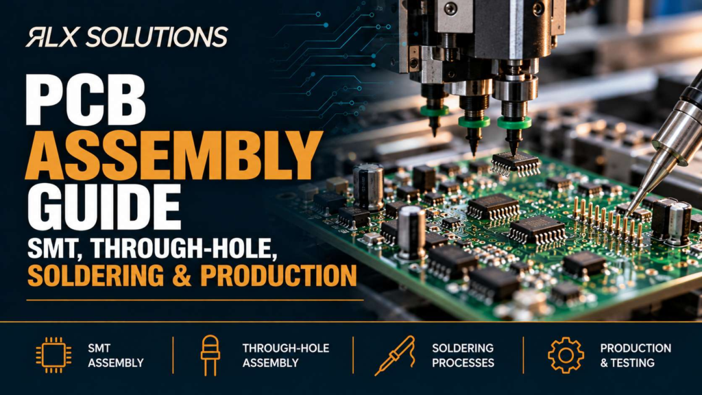
Selective soldering solders specific through-hole joints without exposing the entire printed circuit board to a solder wave. It is particularly useful for mixed-technology assemblies where surface-mount components are already installed. RLX Solutions, a contract electronics manufacturer in Concord, Ontario, uses selective soldering as one assembly process for builds that combine different component technologies.
Selective soldering targets the joints that actually need solder
Selective soldering is an automated through-hole soldering process that applies flux, heat and molten solder to defined locations on a circuit board. Unlike wave soldering, which passes much of the board over a solder wave, selective soldering confines the soldering operation to chosen through-hole leads and pads.
That distinction matters on a mixed-technology assembly. A board may contain hundreds of surface-mount technology (SMT) components but only a few connectors, relays or other through-hole parts. Those parts still require reliable barrel fill and solder-joint formation, but exposing the whole underside of the assembly to a wave can create unnecessary design and process constraints.
Selective soldering changes the problem from “How do we protect everything that should not touch the wave?” to “Can the soldering system reach each required joint and transfer enough heat into it?”
That second question reaches directly into printed circuit board layout.
Consider a hypothetical 6-layer, 1.6 mm board with 220 SMT placements and two 12-pin through-hole connectors along one edge. Only 24 pins require through-hole soldering. Selective soldering can target those locations rather than making the entire underside compatible with a conventional wave process.
The process is selective, but the thermal requirements of a good solder joint remain. The component lead, plated barrel and surrounding pad must reach the conditions needed for solder to wet and fill the joint correctly.
The selective soldering process follows a controlled thermal sequence
A selective soldering cycle is more than touching individual leads with molten solder. Flux application, preheating, solder contact and inspection work together. An error early in that sequence can appear later as poor wetting, incomplete fill, bridging or excess residue.
1. The assembly starts with component placement and support
Through-hole components must be inserted to the correct depth and orientation before soldering. The assembly also needs to remain stable during the soldering cycle.
Lead length, connector seating and mechanical retention matter because movement changes the relationship between the lead, plated hole and soldering location. A connector that sits unevenly can produce inconsistent joint geometry even when the soldering parameters themselves remain unchanged.
The assembly drawing should make component orientation and seating expectations unambiguous.
2. Flux is applied to the selected soldering area
Flux prepares the metal surfaces for solder wetting by helping remove oxides and limiting further oxidation during heating.
Selective application is useful because the process can concentrate flux around joints that will actually be soldered. But location and quantity matter. Too little flux can contribute to poor wetting. Excessive or poorly controlled application can leave unwanted residue or affect nearby areas.
The important manufacturing question is therefore not simply whether flux is present. It is whether the required joint receives appropriate coverage before heating and solder contact.
3. Preheating reduces the thermal jump
Preheating raises the assembly temperature before the soldering operation. This reduces the thermal difference the joint experiences when molten solder reaches the pad and lead.
The effect becomes more important as copper mass increases. A through-hole pad connected to substantial internal copper can remove heat from the joint much faster than an isolated signal connection.
For example, imagine two pins on the same 8-layer board. Pin 1 connects through narrow traces to signal circuitry. Pin 2 connects into large internal copper regions. Their drilled geometry may be identical, but Pin 2 can require substantially more thermal energy because the copper network acts as a heat sink.
That is why through-hole solderability cannot be evaluated from hole diameter alone. Copper connectivity and thermal mass are part of the soldering problem.
4. Molten solder contacts the programmed joints
The soldering stage brings molten solder into controlled contact with the selected leads and pads. The goal is to transfer enough heat and solder to form the required joint without creating problems at neighbouring features.
Access becomes a physical design constraint here. Tall components, tight spacing and nearby bottom-side features can limit the available approach around a through-hole joint.
A layout can therefore be electrically correct yet unnecessarily difficult to solder.
This is one reason design for manufacturability (DFM) should consider assembly processes before the PCB layout is released. Moving a connector or adjusting nearby component placement may be far easier during layout than developing a production workaround after boards and components have been purchased.
5. Cooling, inspection and test close the process
After soldering, joints cool and solidify before inspection. The objective is not simply to confirm that solder is visible. The manufacturer needs evidence that the assembly meets the workmanship requirements specified for the build.
Inspection can include manual visual examination under magnification, while broader PCB assembly inspection may also involve solder paste inspection (SPI), automated optical inspection (AOI) and automated X-ray inspection (AXI) where applicable to other component types on the board.
Electrical testing addresses a different question. A joint can look acceptable yet still sit within a circuit that fails electrically. Conversely, an electrically functioning board still requires the workmanship expected for the specified assembly class.
Inspection and test therefore complement each other rather than serving as substitutes.
Why engineers choose selective soldering over wave or hand soldering
The practical advantage of selective soldering is process isolation. You can solder through-hole components on a populated mixed-technology board without designing every bottom-side feature around full-board wave exposure.
| Decision factor | Selective soldering | Wave soldering | Hand soldering |
|---|---|---|---|
| Solder exposure | Defined through-hole locations | Broad underside exposure | Individual joints |
| Mixed SMT and through-hole boards | Well suited when joints are accessible | Requires greater attention to wave compatibility | Possible, but operator-dependent |
| Repeatability | Program-controlled | Process-controlled across the wave | More dependent on operator technique |
| Layout sensitivity | Access around targeted joints matters | Entire solder-side geometry matters | Physical tool access matters |
| Best process question | Can each target joint be reached and heated correctly? | Can the solder side safely pass over the wave? | Can an operator make each joint consistently? |
Wave soldering can still make manufacturing sense when the underside of the assembly and through-hole population suit that process. Hand soldering also remains useful in appropriate production and rework situations.
Selective soldering becomes compelling when automation is desirable but full-board solder exposure is not.
Board A vs Board B: the layer count does not tell you the soldering difficulty
Take two hypothetical 8-layer, 1.6 mm printed circuit boards. Both use the same layer count and both have a 20-pin through-hole connector.
Board A places the connector near an open board edge. Most pins connect to relatively light signal routing, and the area around the solder-side pads is clear.
Board B places the connector between taller assemblies and routes several pins into large internal copper regions. Nearby bottom-side components reduce physical access around the connector.
The fabrication headline looks nearly identical: 8 layers, 1.6 mm thickness, 20 through-hole pins. The assembly problem is not.
Board B combines greater thermal demand with tighter physical access. That can affect process development, fixture considerations and soldering strategy. A purchasing comparison based only on layer count, board area and component count misses those manufacturing differences.
This is also why two circuit boards with similar bills of materials can carry different assembly effort. The location and thermal environment of the through-hole joints can matter as much as the number of joints.
Selective soldering advantages show up most clearly on mixed-technology boards
The first advantage is controlled exposure. Only the locations intended for through-hole soldering need direct solder contact. That gives PCB designers more freedom to use SMT components elsewhere on the solder side, provided the selective process still has the physical access it needs.
The second advantage is repeatability. Once the manufacturing process is established, programmed movement and controlled process conditions reduce reliance on an operator manually reproducing the same soldering technique across every joint and board.
The third is process control at the joint level. Different areas of a board can present different thermal demands. A connector pin attached to a large copper region does not behave like a lightly connected signal pin. A selective process gives manufacturing engineering a way to address the actual soldering locations rather than treating the whole board as one uniform thermal load.
The fourth is reduced dependence on wave-solder masking and broad underside compatibility. That can matter as assemblies become denser and the number of through-hole components falls while SMT content increases.
None of these advantages eliminates DFM. They make DFM more specific. Access, copper distribution, component geometry and through-hole placement become the variables to review.
Layout decisions can make selective soldering easy or difficult
A selective soldering problem is often created before the assembly reaches production. Component placement and copper design determine whether the soldering operation has enough physical and thermal margin.
Give the soldering operation physical access
A through-hole connector surrounded by tall components may be electrically acceptable but mechanically difficult to reach. Bottom-side SMT components near the target pads can create the same problem.
The manufacturer needs the PCB layout, assembly drawing and component information to evaluate these interactions. A 2D pad pattern alone may not reveal a clearance problem created by the body of an adjacent component.
Account for copper that pulls heat away from the joint
Large planes and heavy copper connections can increase thermal demand at a through-hole joint. The mechanism is straightforward: copper conducts heat away from the pad and plated barrel into the surrounding board.
Thermal relief geometry, where appropriate to the electrical design, can change that heat path. Power integrity and current requirements still come first, so thermal relief should not be added simply to make soldering easier without considering electrical consequences.
This is a design trade-off, not a soldering-machine setting.
Treat hole, lead and pad geometry as one system
A plated through-hole joint depends on the relationship among the component lead, finished hole and pad. Changing one changes the volume and geometry available for solder.
For a hypothetical connector, suppose one design uses a 0.8 mm lead in a 1.0 mm finished hole while a redesign substitutes a component with a different lead geometry. Even if the PCB footprint appears similar on screen, the soldering behaviour can change because the lead-to-hole relationship has changed.
That is why component substitutions deserve assembly review rather than being treated solely as bill-of-material changes.
Common selective soldering defects have identifiable mechanisms
Incomplete or inconsistent joints are usually symptoms of a process or design condition. Finding the mechanism matters more than simply reworking the visible defect.
Insufficient wetting can occur when surfaces do not wet properly during the available thermal cycle. Surface condition, flux performance and heat transfer all matter.
Incomplete barrel fill can appear when the solder and joint do not receive the thermal conditions needed for proper flow through the plated hole. High copper mass can make this harder because heat is conducted away from the soldering location.
Bridging occurs when solder connects conductors that should remain electrically separate. Pad spacing, lead geometry and process conditions can influence the risk.
Component movement during soldering can disturb joint formation. Mechanical seating and support therefore belong in the process discussion, especially for larger connectors and components.
Heat-sensitive neighbouring features can restrict the process window even though they are not themselves being soldered. Selective soldering reduces broad solder exposure, but heat still moves through the PCB and nearby materials.
A useful failure analysis therefore looks beyond the defective joint. It asks what the copper structure, component geometry, access conditions and process sequence were doing at that location.
Applications that benefit from selective soldering
Selective soldering is most relevant where through-hole components remain necessary on an otherwise surface-mount-heavy assembly.
Connectors are a common example because mechanical requirements can favour through-hole termination. Relays, switches and other electromechanical parts can create similar assembly needs. Mixed-technology boards may also use through-hole components where mechanical retention, package availability or electrical requirements make them appropriate.
Consider a hypothetical 4-layer controller with a 0.5 mm pitch SMT device, dozens of chip components and three through-hole connectors. Reflow can handle the SMT population first. Selective soldering can then address the connector pins without requiring the whole populated underside to interact with a solder wave.
A second application is a board where through-hole components are concentrated in a few defined areas. If 95 per cent of the assembly is SMT and the remaining joints sit in two connector banks, targeted soldering can match the physical distribution of the work.
The decision becomes less attractive when the required joints are physically inaccessible to the process or when the entire solder side is already well suited to wave soldering. Process selection should follow the assembly geometry rather than a preference for one soldering method.
Inspection requirements should follow the finished assembly
Selective soldering does not operate in isolation from the rest of PCB assembly. A mixed-technology board may pass through solder paste printing, SMT placement, reflow, through-hole insertion, selective soldering, inspection and electrical test before release.
That sequence creates several inspection points with different purposes.
SPI evaluates solder paste before reflow. AOI examines post-reflow assembly features. AXI can examine packages such as ball grid arrays (BGAs), land grid arrays (LGAs) and quad flat no-lead (QFN) devices where relevant. Manual visual inspection evaluates workmanship under magnification. In-circuit and functional testing then address electrical behaviour according to the production test strategy.
For IPC-A-610 Class 2 or Class 3 builds, the workmanship level specified by the customer also affects acceptance expectations. Class 3 applies tighter workmanship requirements than Class 2. The assembly documentation should therefore identify the required class rather than leaving production to infer it from the product type.
First article inspection (FAI) is particularly valuable on a new mixed-technology build because it creates a controlled point to verify the assembled product before the production lot proceeds.
Send manufacturing data that exposes the real soldering problem
A manufacturer cannot properly assess selective soldering from a bill of materials (BOM) alone. The BOM identifies parts, but it does not show where those parts sit, what surrounds them or how the target joints connect into the board.
For PCB assembly, the useful manufacturing package includes:
- BOM in .xlsx or .csv format. This establishes the specified components and helps identify the through-hole population.
- Pick-and-place or centroid data. This defines component locations for automated assembly planning.
- Assembly drawing. This communicates orientation and assembly-specific requirements that may not be obvious from raw coordinate data.
- PCB manufacturing data. Gerber RS-274X, ODB++ or IPC-2581 data, with NC drill information, exposes the physical circuit board geometry.
- Stackup and fabrication documentation where relevant. Copper distribution and board construction can help explain why apparently similar through-hole joints present different thermal conditions.
- Workmanship and test requirements. The manufacturer needs to know the required build class and what functional or electrical verification is expected.
File completeness affects more than quoting. It allows manufacturing engineering to catch a connector-access problem or unusual thermal condition before assembled hardware reaches the soldering stage.
Selective soldering belongs in DFM before production starts
Selective soldering works best when the PCB is designed with the soldering operation in mind. Waiting until assembled boards reach the line turns layout constraints into manufacturing problems.
For a new mixed-technology build, review the through-hole population, solder-side component placement, connector seating, copper connectivity and required inspection strategy together. That gives the manufacturer enough context to determine whether selective soldering fits the assembly and where process development may be required.
If you are preparing a mixed-technology circuit board for production, RLX reviews design for manufacturability and design for assembly as part of every quote. Send the Gerbers or other accepted manufacturing data, BOM, pick-and-place file and assembly drawing so the through-hole strategy can be reviewed with the complete assembly rather than as an isolated soldering operation.
Frequently Asked Questions
Can selective soldering be used after SMT reflow?
Yes. Selective soldering is particularly useful on mixed-technology assemblies where SMT components are installed through the reflow process and selected through-hole components still require soldering. The board layout must provide suitable access to the target joints, and the thermal effect on the populated assembly needs to be considered during manufacturing planning.
Does selective soldering replace wave soldering?
Not universally. Selective soldering targets defined through-hole locations, while wave soldering exposes a broader area of the solder side to molten solder. A board with a small number of through-hole components among a large SMT population may favour selective soldering. A design with extensive wave-compatible through-hole content can present a different manufacturing case.
Is selective soldering better than hand soldering?
They solve different production problems. Selective soldering provides a programmed process for targeted joints, which can improve repeatability across recurring builds. Hand soldering can remain appropriate for certain assembly or rework tasks. The choice should consider joint count, physical access, thermal behaviour, workmanship requirements and the expected production process.
What files are needed to quote a mixed-technology PCB assembly?
A complete PCB assembly package should include a BOM, pick-and-place or centroid file and assembly drawing, along with the required PCB manufacturing data. Gerber RS-274X, ODB++, IPC-2581 and NC drill files are accepted manufacturing formats. Supplying the complete package allows assembly and fabrication requirements to be reviewed together.
Can selective soldering be used for IPC-A-610 Class 3 assemblies?
Selective soldering can be part of assemblies built to IPC-A-610 Class 3 workmanship requirements. The specified class affects workmanship and acceptance expectations rather than defining one mandatory soldering process. Inspection, documentation and test planning should therefore be established around the finished assembly and its specified requirements.
How should engineers prepare a board for selective soldering?
Start with physical access and thermal behaviour. Identify every through-hole joint that requires soldering, check nearby solder-side components and tall mechanical features, and examine connections into substantial copper areas. Provide complete manufacturing and assembly data so these conditions can be evaluated during engineer-reviewed DFM rather than after boards have entered production.