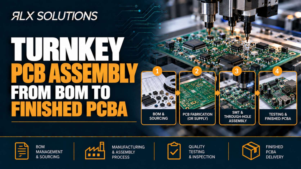
Turnkey PCB assembly puts component procurement, bare-board supply, assembly,
inspection and test under one manufacturing programme instead of splitting
them among vendors. RLX Solutions, a contract electronics manufacturer in
Concord, Ontario, uses this model to turn an approved BOM and manufacturing
package into a finished printed circuit board assembly ready for shipment.
The convenience is easy to describe. The engineering consequence matters more.
A turnkey contract manufacturer is responsible for coordinating decisions
that affect each other: whether the bill of materials can actually be sourced,
whether substitutes change assembly risk, whether the printed circuit board
stackup supports the package geometry, whether moisture-sensitive parts are
handled correctly, and whether the inspection plan can see the defects the
design is likely to produce.
That coordination is what separates turnkey PCB assembly from simply buying
parts and placing them.
Turnkey PCB assembly starts with the manufacturing package
A bill of materials (BOM) tells the manufacturer what components belong on
the board, but it is not enough to manufacture the assembly by itself. The
assembly programme also needs the files that define the bare circuit board,
component locations, orientation and production requirements.
For a complete PCB assembly package, that normally means:
- BOM in .xlsx or .csv format
- Gerber RS-274X, ODB++ or IPC-2581 fabrication data
- NC drill files
- Pick-and-place or centroid data
- Assembly drawing
- Stackup information where relevant
- Impedance targets where controlled impedance is required
- Fabrication notes and assembly notes
An engineer-reviewed design for manufacturability and design for assembly
(DFM/DFA) review matters here because discrepancies tend to propagate. If the
BOM calls for a 0.5 mm pitch device but the centroid data uses an outdated
footprint revision, purchasing may acquire the correct part while assembly
receives incorrect placement data.
Version control therefore becomes a manufacturing issue, not an administrative
one. The BOM, PCB fabrication data, assembly drawing and placement file need
to describe the same revision.
Worked example: one wrong revision can cross three departments
Consider an eight-layer board that has been revised from a 0.8 mm pitch BGA
to a 0.5 mm pitch replacement.
Revision A of the BOM lists the old BGA. Revision B lists the replacement.
The PCB layout was updated for Revision B, but the pick-and-place file was
accidentally exported from Revision A.
The bare board may fabricate correctly. Procurement may also buy the intended
Revision B device. The problem appears during programming, placement review
or first article inspection because the manufacturing files disagree.
Turnkey assembly reduces the number of commercial handoffs, but it does not
remove the need for disciplined release control. A manufacturer still needs
one coherent package before procurement and production begin.
Component procurement is part of the engineering risk
Turnkey assembly means the manufacturer procures the components rather than
waiting for a customer-supplied kit. That shifts more responsibility upstream,
where availability, date codes, packaging condition and authenticity can
affect whether the board reaches the line at all.
Authorized distribution is usually the cleanest sourcing path because
provenance is easier to establish. Supply constraints, obsolete devices or
end-of-life parts can require other channels, including vetted independent
distribution, excess inventory or global sourcing networks.
The important distinction is not simply where the part was bought. It is how
the source and the material are verified.
A counterfeit-prevention workflow can include source vetting, packaging
inspection, checking date code and country-of-origin information, visual
inspection to IDEA-STD-1010 criteria, lot verification, X-ray examination,
electrical testing and, where risk warrants escalation, third-party
decapsulation and die analysis.
That process becomes especially relevant when a BOM contains an obsolete
microcontroller, allocated power device or legacy connector that cannot be
obtained through normal authorized channels.
Moisture-sensitive devices add another requirement. Packaging condition,
dry storage and handling need to be controlled according to IPC/JEDEC
J-STD-033 practices so a genuine component is not damaged before it is even
placed.
Bare PCB fabrication can change the assembly plan
Turnkey PCB assembly does not begin at the placement machine. The bare PCB
is the mechanical and electrical foundation for every solder joint that
follows.
Board stackup, copper weight, via architecture, surface finish, solder mask
geometry and controlled impedance requirements all influence fabrication.
Several of those choices also change what assembly inspection needs to verify.
For example, a design using via-in-pad plated over fill places filled, capped
and planarized vias directly beneath component pads. That may be useful for
dense ball grid array (BGA) fanout, but the fabrication process has to produce
a flat solderable pad before solder paste is printed.
Blind vias create another dependency. On a four-layer or greater stackup,
blind-via construction requires sequential lamination. If the designer decides
late in the release cycle to replace through vias with Layer 1 to Layer 2
blind vias, the change is not just a drill-file update. It changes how the
bare board is built.
Aspect ratio also matters for mechanically drilled plated holes. As board
thickness rises or finished-hole diameter falls, plating becomes harder to
maintain through the full barrel. A fabrication review therefore has to
consider hole geometry and board thickness together rather than treating
minimum drill size as an isolated number.
Board A versus Board B: same layer count, different manufacturing cost
Consider two hypothetical 10-layer, 1.6 mm printed circuit boards of the
same overall dimensions.
| Decision factor | Board A | Board B |
|---|---|---|
| Layer count | 10 layers | 10 layers |
| Via structure | Through-hole vias | Layer 1 to 2 microvias, Layer 2 to 3 microvias and buried inner-layer vias |
| Smallest via type | Mechanically drilled PTH | 0.10 mm laser-drilled microvias |
| Lamination | Conventional multilayer build | Sequential lamination |
| BGA fanout | Through-via fanout | HDI fanout |
| Via-in-pad | No | Filled, capped and planarized pads in selected BGA area |
| Fabrication consequence | Fewer build stages | More drilling, filling, plating and lamination operations |
| Assembly consequence | Conventional paste-printing surface | Pad planarity becomes important beneath the BGA |
The layer count is identical, but Board B contains more manufacturing stages
and more interfaces where variation can enter.
That is why PCB assembly pricing cannot be inferred from layer count alone.
The stackup and interconnect architecture determine how difficult the bare
board is to manufacture before a component reaches it.
Solder paste inspection catches problems before reflow
Surface-mount assembly begins with solder paste deposition through a stencil.
For dense assemblies, the amount and position of paste can determine whether
a solder joint ever has a chance to form correctly.
Solder paste inspection (SPI) measures paste volume, area and offset before
the components enter reflow. Checking paste before reflow is important because
a downstream inspection system can identify a solder defect, but it cannot
recover the production time already spent placing and reflowing a bad print.
This becomes more significant as pad dimensions shrink.
Imagine a board carrying 01005 passives and a 0.3 mm pitch BGA. The assembly
process is now sensitive to small changes in paste deposition, pad alignment
and component placement. A print problem repeated across a panel can create
dozens of downstream defects from one upstream cause.
SPI therefore works as process control, not just defect detection.
Placement and reflow convert the bare board into a PCBA
Once paste deposition is verified, surface-mount technology (SMT) components
are placed according to the centroid data and assembly programming. The
populated board then passes through reflow so the solder paste forms
metallurgical joints between component terminations and PCB pads.
A printed circuit board assembly, commonly shortened to PCBA, is the populated
board after electronic components have been attached. Mixed-technology
assemblies may combine SMT with through-hole parts, press-fit components or
selective soldering.
Package geometry changes how much of the resulting connection can be inspected
visually.
A chip resistor exposes its solder joints around the perimeter. A BGA hides
its joints beneath the package. A quad flat no-lead (QFN) package may include
a large thermal pad that is also hidden once the device is placed.
That difference determines the inspection method required after reflow.
Inspection needs to match the package, not just the board
Automated optical inspection (AOI) is useful after reflow for visible
placement and solder conditions on both sides of the PCB. It can identify
issues such as missing parts, polarity errors and visible solder-joint defects.
AOI cannot directly see a solder joint hidden beneath a BGA or land grid array
(LGA). Automated X-ray inspection (AXI) addresses that blind spot by examining
internal solder features, including BGA and LGA joints and QFN thermal pads.
The mechanism matters. Optical inspection evaluates light reflected from
visible features. X-ray imaging evaluates density through the assembly.
Hidden-joint packages therefore require a different observation method.
For a board with a 0.3 mm pitch BGA, inspection strategy should be decided
before production rather than after a failure appears. Package selection and
test coverage are connected design decisions.
Manual visual inspection still has a role. Boards can be inspected under
magnification against IPC-A-610 Class 2 or Class 3 workmanship requirements,
depending on the programme.
Class 3 does not simply mean that an inspector looks harder. It applies
tighter workmanship expectations and documentation requirements, so the build
class should be agreed before manufacturing documentation and acceptance
criteria are finalized.
First article approval creates a controlled production baseline
The first article is the first completed build used to verify that the released
files, materials and manufacturing process produce the intended assembly.
This is the point where a programme can catch a systematic error before the
full lot follows it.
Suppose a 200-board order contains a polarized connector rotated 180 degrees
in the assembly drawing while the PCB silkscreen and design database show the
intended orientation. If production begins without resolving that conflict,
the same error can be repeated across the lot.
A first article inspection (FAI) interrupts that path. On a new build, the
initial assembly can be reviewed and customer approval obtained before
production lot release.
The economic value is straightforward. Discovering one systemic issue on the
first unit is different from discovering the same issue after 200 units have
been assembled.
Electrical test answers a different question from visual inspection
Inspection asks whether the board appears to have been manufactured correctly.
Electrical test asks whether its electrical network or intended functions
behave correctly.
Those are related but separate questions.
Flying-probe in-circuit test (ICT) is suited to prototype and lower-volume
work because it can contact test points without a dedicated bed-of-nails
fixture. It can provide full net coverage where the board has been designed
for the required access.
At production volume, bed-of-nails ICT can use a dedicated fixture to make
simultaneous electrical contact across the board.
Functional test (FCT) moves beyond connectivity. It exercises the assembly
according to a customer-defined specification and records pass or fail
results. Depending on the product, that may involve powering rails,
communicating with interfaces, operating loads, verifying programmed
functions or checking sensor behaviour.
A board can pass AOI and still fail electrically. It can also pass continuity
checks while failing its intended function. Inspection, ICT and FCT therefore
answer different failure questions.
Programming, serialization and finishing belong in the build plan
Many finished assemblies require work after soldering and inspection.
In-system programming can load firmware through interfaces such as JTAG, SWD,
ISP or ICSP. Programming can also include bootloader installation or firmware
flashing.
Serialization associates a physical assembly with a unique identity. Serial
marking, programmed MAC addresses, labels or laser marks can then connect
that board to production and test records.
Those steps matter when troubleshooting moves from the production line into
field service. If a failed unit can be tied back to its material lots,
programmed configuration and test results, failure analysis starts with
evidence rather than reconstruction.
Other post-assembly processes can include conformal coating, underfill,
potting, encapsulation, press-fit insertion, selective soldering and BGA
rework. These should be specified before production because they affect
routing through the factory.
For example, conformal coating applied after electrical test creates a
protective layer over the completed assembly. If a board will later require
connector mating, probe access or adjustment, those keep-out areas must be
defined before coating.
Turnkey, kitted and consigned assembly solve different sourcing problems
Turnkey PCB assembly is one of three common material models.
| Decision factor | Turnkey | Kitted or partial turnkey | Consigned |
|---|---|---|---|
| Component purchasing | Manufacturer buys the BOM | Customer supplies selected parts, manufacturer buys the rest | Customer supplies the complete kit |
| Bare PCB | Manufacturer fabricates or sources | Programme-dependent | Programme-dependent |
| Best fit | Customer wants one accountable manufacturing programme | Customer controls critical or long-lead items | Customer already owns the complete material set |
| Main coordination issue | Supplier manages sourcing and production dependencies | Ownership must be clear for every BOM line | Kit completeness and material condition become central |
| Buyer workload | Lowest material-management burden | Shared | Highest pre-build material responsibility |
Turnkey is strongest when the objective is to transfer component purchasing
and production coordination to the contract manufacturer.
Partial turnkey makes sense when the customer must control selected
components. A design team might, for example, consign a programmed security
device or a scarce processor while asking the manufacturer to procure standard
resistors, capacitors, connectors and the remaining BOM.
Consigned assembly shifts sourcing responsibility back to the customer. That
can be useful when material is already owned, but a missing reel or mismatched
quantity can stop the build because the assembler cannot simply treat the BOM
as a purchasing requirement.
The decision therefore concerns ownership of material risk as much as
purchasing convenience.
A complete quote should expose manufacturing dependencies early
Turnkey PCB assembly works best when commercial quoting and engineering review
happen from the same release package.
A low component price does not help if the chosen alternate changes package
geometry. A low bare-board price does not help if a surface finish is poorly
matched to the assembly process. A fast component purchase does not help if
the fabrication data still contains unresolved stackup questions.
For procurement teams, this is where the contract manufacturing model earns
its value. One programme owner can coordinate BOM sourcing, PCB fabrication,
assembly, first article review, inspection and test without forcing the buyer
to reconcile separate supplier assumptions.
For engineers, the requirement is equally practical: release enough
information for those dependencies to be reviewed before purchase orders
lock them in.
What to send for a turnkey PCB assembly quote
If the goal is a quote that can progress into manufacturing without a second
documentation cycle, send the complete release package rather than the BOM
alone.
Include the BOM, fabrication data, NC drill, pick-and-place file and assembly
drawing. Add the stackup and impedance requirements where they apply, and
include fabrication or assembly notes that affect acceptance.
Also identify the required workmanship class and provide the functional test
specification if FCT is part of the programme.
If programming is required, include the firmware package and programming
instructions. If serial numbers, MAC addresses or labels must follow a
particular format, define that before the first article.
These inputs let the manufacturer review the board as a manufacturing system
rather than as disconnected purchasing and assembly tasks.
From files to a production-ready build
If you are preparing a turnkey build, RLX reviews the manufacturing package
as part of every quote. Send the Gerbers or other accepted fabrication data,
BOM, pick-and-place file and assembly drawing so sourcing, bare-board
fabrication, assembly requirements and engineer-reviewed DFM/DFA feedback can
be evaluated together.
Frequently Asked Questions
What does turnkey PCB assembly include?
Turnkey PCB assembly means the manufacturer procures the components,
fabricates or sources the bare PCBs, assembles the boards, performs the
specified inspection and test, and ships the completed assemblies. The
customer supplies the design and manufacturing package rather than sourcing
and shipping every production component as a complete kit.
What files are needed for turnkey PCB assembly?
A complete package normally includes the BOM, Gerber RS-274X, ODB++ or
IPC-2581 fabrication data, NC drill files, pick-and-place or centroid data
and an assembly drawing. Stackup information, impedance targets, fabrication
notes, programming files and functional test requirements should also be
supplied when they apply to the design.
Can a turnkey manufacturer source obsolete electronic components?
Yes. Obsolete and end-of-life components can be sourced through channels
beyond current authorized distribution, including excess inventory and
specialised sourcing networks. The sourcing route should be paired with an
authenticity plan that can include source vetting, packaging checks,
IDEA-STD-1010 visual inspection, X-ray, electrical testing and further
analysis where required.
What is the difference between AOI and X-ray inspection?
Automated optical inspection checks visible component placement and solder
features after reflow. X-ray inspection can evaluate solder connections
hidden beneath packages such as BGAs and LGAs and can examine QFN thermal
pads. A board with hidden-joint packages therefore requires inspection
coverage that does not rely on visible solder fillets alone.
Do I need functional testing if the board already receives ICT?
They serve different purposes. In-circuit testing checks electrical networks
and can detect issues such as opens or shorts. Functional testing operates
the assembly against a customer-defined specification and records whether
the intended functions work. A board can have correct net connectivity yet
still fail firmware, interface, power or system-level behaviour.
When should I choose partial turnkey instead of full turnkey?
Partial turnkey is useful when you need to retain control of selected
components while asking the manufacturer to source the remainder of the
BOM. Typical reasons include customer-owned inventory, scarce parts or
devices that require programme-specific control. The important step is
assigning sourcing responsibility clearly to every BOM line before
purchasing starts.