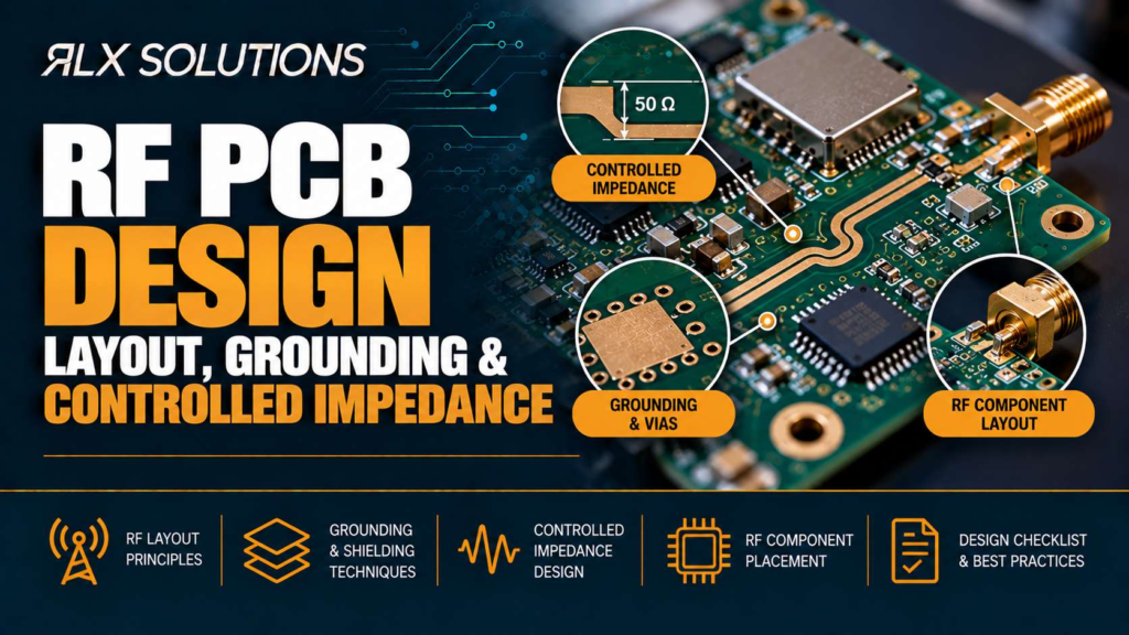
RF PCB design succeeds when the stackup, transmission-line geometry, return path and fabrication process are treated as one electrical system. RLX Solutions, a contract electronics manufacturer in Concord, Ontario, approaches RF layout from that manufacturing reality: the impedance calculation is useful only if the finished circuit board can reproduce the geometry on which it depends.
Start RF PCB Design With the Stackup, Not the Trace Width
An RF trace does not have an impedance because a layout tool labels it “50 ohms.” Its characteristic impedance comes from the electromagnetic field created by a specific conductor geometry and its surrounding dielectric and reference conductors.
For a surface microstrip, the important variables include trace width, finished copper thickness, distance to the reference plane and laminate properties. A stripline adds another reference plane and changes field confinement. Grounded coplanar waveguide adds adjacent grounded copper and the gap to that copper as another design variable.
That makes stackup selection an electrical decision. Changing the dielectric thickness after routing can force a different trace width. Changing copper weight alters the finished conductor geometry. Moving the reference plane changes both impedance and return-current behaviour.
A practical sequence is:
- Define the transmission-line impedance and RF frequency range.
- Select the signal layer and its reference plane.
- Establish laminate, copper and dielectric construction.
- Calculate the required trace geometry from that construction.
- Route with the geometry held consistent through bends, pads and transitions.
- Release the impedance target with the stackup and fabrication data.
Controlled impedance means manufacturing the transmission line so its finished geometry produces the specified characteristic impedance within an agreed tolerance. For fabrication, that turns impedance from a schematic requirement into a dimensional process requirement.
Worked example: the same 50-ohm target can require different geometry
Consider a hypothetical 6-layer RF board with its main RF route on Layer 1 and a solid reference plane on Layer 2. The design target is 50 ohms.
In the first proposed stackup, Layer 1 sits 0.10 mm above Layer 2. In a second stackup, that spacing is increased to 0.20 mm while the laminate system and copper construction remain otherwise comparable.
You cannot safely retain the first trace width and assume the second board is still a 50-ohm structure. Doubling the separation changes the field geometry. The transmission-line dimensions need to be recalculated before layout release.
This is why substituting a “standard” stackup after routing can create an RF problem without changing a single net in the CAD database.
Give Every RF Trace a Continuous Return Path
RF grounding is primarily return-path engineering. The signal current and its high-frequency return current form a coupled electromagnetic structure, so a trace should be considered together with the reference plane underneath or around it.
With a surface RF trace referenced to Layer 2, the return current tends to concentrate near the trace on that plane. A slot, plane split or large clearance region below the route forces the current away from its preferred path.
The electrical consequence is a larger loop. Loop inductance rises, fields spread farther from the route, coupling can increase and the transmission-line impedance becomes less predictable around the discontinuity.
That is why a solid ground reference generally matters more than drawing an arbitrary ground boundary around an RF section.
Plane splits are electrical obstacles, not drawing features
Suppose a 2.4 GHz route runs on Layer 1 from a transceiver to a matching network. Layer 2 is its ground reference. Halfway along the route, a wide plane clearance interrupts Layer 2.
The Layer 1 copper may remain perfectly straight, but the electromagnetic path is not straight. Return current has to flow around the opening before returning beneath the trace.
Moving the Layer 1 route so it remains entirely above continuous Layer 2 copper preserves a much cleaner return path without adding any component or changing the schematic.
The same principle applies near connector launches, mounting holes, plane cut-outs and dense via fields. Review what exists under the RF line, not just what exists beside it.
Controlled Impedance Has to Survive the Whole RF Route
A controlled-impedance trace is useful only while the transmission-line structure remains reasonably consistent. The weak points are often transitions rather than long, straight sections.
Watch the geometry at:
- component pads and matching networks
- RF connectors and launches
- neck-down sections
- test pads and branches
- signal vias and their anti-pads
- layer changes
- transitions between microstrip and stripline
- grounded coplanar structures where the ground gap changes
A short discontinuity may appear insignificant in the layout view, but RF energy responds to changes in capacitance and inductance. A wide pad can behave as excess capacitance. A narrow section can add inductive behaviour. A via adds a three-dimensional transition whose unused portion may behave differently from the routed transmission line.
This is also why the shortest geometric route is not always the best route. A slightly longer path that preserves its reference plane and transmission-line geometry can be electrically cleaner than a shorter path containing two layer changes and a plane discontinuity.
Treat vias as part of the transmission line
When an RF net changes layers, the signal via is only one part of the transition. The return current also needs a path from the original reference plane to the new reference plane.
For example, consider an 8-layer board where an RF trace begins as Layer 1 microstrip referenced to Layer 2, then moves to Layer 6 and is referenced to Layer 7. The signal via connects the copper route, but the reference transition must also be considered.
Nearby ground vias can provide an RF return connection between the reference structures. Without an appropriate return transition, the signal changes layers while its return current is forced to find a longer route through the board.
Via pad diameter, anti-pad geometry, drill size, board thickness and unused via length can all affect the transition. At higher frequencies, the transition may need to be treated as an RF structure rather than as a generic routing via.
Ground Stitching Controls Where the RF Field Can Travel
Ground stitching vias connect ground copper on different layers and reduce the inductive distance between those conductors. They become especially relevant around grounded coplanar waveguide, RF launches, board edges, shielding regions and layer transitions.
Spacing should come from the electrical behaviour you are trying to control rather than from a cosmetic grid.
For a grounded coplanar line, for example, the side ground pours are useful only if they remain effectively tied to the reference ground structure. Widely separated stitching connections can allow sections of copper to behave differently from the intended RF boundary.
The manufacturer also needs enough physical space to drill and plate those vias without violating pad, clearance or fabrication requirements. A stitching pattern therefore has to satisfy both RF intent and PCB manufacturing geometry.
Do not add ground vias until every open area is filled with them. Each hole consumes routing area, creates clearances on other layers and can interfere with power or signal structures. Place them where they perform an identifiable return-path, shielding or field-containment function.
RF Material Selection Starts With Loss and Stackup Geometry
Material choice affects more than the value entered for dielectric constant in a calculator. Laminate electrical properties, dielectric construction and the physical stackup determine transmission-line behaviour, while material loss contributes to attenuation along the route.
A conventional FR-4 construction can make sense for many boards, while higher-frequency or lower-loss requirements can lead to RF laminate systems. Available fabrication materials can include high-Tg FR-4 as well as high-frequency materials such as Rogers RO4003C, RO4350B, RO3003 and RO3010, Taconic RF materials, Arlon materials, PTFE-based constructions and Panasonic MEGTRON.
The engineering question is not “Is this an RF board?” It is whether the frequency, insertion-loss budget, route length, thermal requirements and transmission-line structure justify the material system.
Changing laminate late in the design creates a second problem: the impedance geometry may also change. A material substitution should therefore trigger a transmission-line and stackup review rather than being treated as a procurement-only decision.
Hybrid construction can create another interface to engineer
A board may need RF material only in part of its layer structure while the remaining layers serve power, control or digital functions. That can make a hybrid construction attractive, but the final stackup still has to satisfy lamination, thickness and impedance requirements together.
For the layout engineer, the key point is simple: specify the electrical result and release the actual stackup used to obtain it. Do not detach the impedance drawing from the material definition that made the dimensions valid.
Board A vs Board B: Layer Count Does Not Predict RF Fabrication Cost
Two boards can both be 10-layer designs and require very different manufacturing sequences.
| Decision factor | Board A | Board B |
|---|---|---|
| Layer count | 10 layers | 10 layers |
| RF routing | Layer 1 referenced to Layer 2 | Layer 1 plus internal RF transitions |
| Via structure | Plated through-holes | Layer 1 to Layer 2 microvias plus internal buried vias |
| RF transition count | Low | Multiple |
| Lamination sequence | Conventional multilayer construction | Sequential processing required by blind or buried structures |
| Via finishing | Conventional PTH | Selected filled or capped structures may be required |
| Manufacturing impact | Fewer process stages | More drilling, lamination and registration operations |
The reason Board B can cost more is not the number “10.” It is the process sequence created by the via architecture.
Assume both hypothetical boards are 1.6 mm thick. Board A routes its 50-ohm RF lines on Layer 1 and uses ordinary through vias outside the critical RF path. Board B must escape a dense device using 0.10 mm Layer 1 to Layer 2 laser-drilled microvias, then connect inner circuitry through buried vias before final lamination.
Board B adds operations before the finished board even reaches the same final layer count. If via-in-pad is used under a fine-pitch RF device, resin filling, copper capping and planarization can add another manufacturing requirement.
This is why RF and high-density interconnect decisions should be made together. A layer transition chosen to shorten an RF route may change the fabrication architecture of the entire printed circuit board.
Keep Matching Networks Physically Honest
An RF matching network exists in a physical transmission path. Component placement therefore affects the electrical network represented by the schematic.
Long connections between a series component and the RF line introduce additional interconnect. A shunt component connected to ground through a long, narrow route or distant via adds inductance in a location where the schematic may show an ideal ground.
The practical layout objective is to make the physical current path resemble the intended RF network as closely as the package and fabrication rules allow.
For a pi network, that means thinking through:
- where the transmission line enters the network,
- the pad geometry at each series element,
- the ground path from each shunt element,
- the transition back into the controlled-impedance route.
Do not automatically convert every pad-to-pad segment into the nominal transmission-line width. The component land pattern itself creates a discontinuity, and very short interconnects around a matching network may need to be analysed as part of the complete structure.
This is one area where schematic connectivity is an incomplete description of RF performance.
Separate RF Isolation Problems From Ground-Splitting Problems
Mixed-signal circuit boards often contain RF, digital, clock, switching-power and low-level analogue sections. Isolation between them is necessary, but cutting the ground plane is not automatically the correct method.
A split can remove the continuous return path required by the very signal you were trying to protect.
Physical placement is usually the first control. Keep noisy switching nodes away from sensitive RF inputs. Keep clock routing out of antenna and front-end regions. Orient functional blocks so that high-current or fast-edge paths remain local.
Then route each signal over an appropriate, continuous reference structure.
The useful distinction is between separating sources and routes and separating their RF return plane. Those are different actions. You can create substantial physical isolation while retaining the ground continuity required for predictable transmission lines.
Design RF Connector Launches as Transitions
A connector interface joins at least two electromagnetic structures: the PCB transmission line and the connector. Mechanical fit alone does not guarantee a clean RF launch.
Pad dimensions, ground placement, anti-pad geometry and reference-plane location all affect the local impedance. Edge-launch connectors add the board edge and finished thickness to the geometry. Vertical connectors introduce their own signal and ground via fields.
This is a good place to avoid generic land-pattern thinking. The connector manufacturer’s recommended footprint may provide a useful starting structure, but it still has to be reconciled with the board’s actual stackup.
If the recommended launch assumes a different dielectric height or board thickness, copying only the copper pattern separates the footprint from the electromagnetic conditions under which it was developed.
Controlled Impedance Must Be Defined in the Fabrication Package
A fabricator cannot infer your intended impedance from a trace that happens to be a certain width.
The fabrication package should make the relationship explicit. Useful manufacturing data includes:
- finished stackup
- controlled-impedance target
- nets or impedance classes to which the target applies
- intended transmission-line layer
- applicable reference plane
- copper construction
- material definition
- Gerber RS-274X, ODB++ or IPC-2581 data
- NC drill data
- fabrication notes
An impedance drawing and stackup PDF can prevent ambiguity that is difficult to reconstruct from copper artwork alone.
Fabrication can support controlled impedance to ±10%, with tighter than ±5% requiring project-specific confirmation. Time-domain reflectometry (TDR) on a coupon can be used to verify the manufactured impedance, with the test report supplied with the order.
A TDR coupon is a representative transmission-line structure placed on the fabrication panel so impedance can be measured without probing a functional RF route on the finished product. Its usefulness depends on the coupon representing the relevant board construction.
That final point matters. Impedance verification does not rescue an incorrect design target. It tells you whether manufacturing produced the specified structure.
DFM Review Should Happen Before RF Geometry Is Frozen
RF design for manufacturability (DFM) should test the electrical assumptions against the fabrication process while changes are still inexpensive.
A useful review looks at the stackup, transmission-line geometry, copper weights, drill structure, via aspect ratio, material selection, reference planes and controlled-impedance definitions as one system.
Consider a hypothetical 12-layer, 2.4 mm-thick board with a proposed 0.20 mm plated through-hole. Its nominal depth-to-drill relationship is already something the fabricator needs to assess before the layout relies on thousands of identical holes. Moving an RF transition to a blind via may solve one electromagnetic problem but create a sequential-lamination requirement.
The objective is not simply to ask whether each feature can be fabricated independently. It is to determine whether they form a manufacturable stackup together.
That becomes especially important with laser-drilled microvias, blind and buried vias, via-in-pad structures, high-frequency laminates and tightly constrained impedance geometries. These decisions interact with registration, lamination and plating long before assembly begins.
Release RF Layout With Measurement in Mind
An RF board should be designed so the eventual measurements answer useful questions.
If an RF path contains a connector launch, matching network, layer transition and antenna interface, debugging is easier when the engineer can distinguish those structures rather than treating the entire route as one unknown.
Test access has a trade-off. A poorly placed test pad can become an RF discontinuity, while removing all access can make characterization harder. Decide what must be measured before adding a branch or pad to a controlled transmission line.
The same thinking applies to fabrication verification. Impedance coupons and TDR reports answer whether the manufactured transmission-line structure matches the specified target. Functional RF measurements answer a different question: whether the assembled system meets its electrical requirements.
Fabrication control and functional validation complement each other. They are not substitutes.
Prepare the RF Design for Fabrication Before Release
If you are moving an RF circuit board from layout into prototype or production, RLX can review the stackup, impedance requirements and manufacturing files as part of an engineer-reviewed DFM process. Release the actual material assumptions, controlled-impedance targets, Gerbers or intelligent manufacturing data, NC drill files and stackup documentation together so electrical intent survives the handoff.
FAQ
What is the best grounding method for an RF PCB?
Use a continuous reference plane for the RF transmission line and keep the high-frequency return path close to the signal path. Avoid routing critical RF traces across plane splits or voids. Where signals change reference layers, provide an appropriate ground-return transition. Ground stitching can then be used where it supports field containment, connector launches or coplanar structures.
Does every RF trace need controlled impedance?
No. Controlled impedance is most relevant when a conductor behaves as a transmission line and reflections or matching affect system performance. Short connections inside lumped matching networks may need different treatment from a long RF feed line. The decision should follow frequency, physical length, loading and the electrical function of the interconnect rather than an “RF net” label alone.
Should I use microstrip or stripline for RF routing?
Microstrip places the conductor on an outer layer with a nearby reference plane, making component and connector access straightforward. Stripline embeds the conductor between reference planes, giving stronger field confinement but requiring internal routing and transitions to surface components. Choose the structure from loss, isolation, transition count, stackup and routing requirements rather than from impedance alone.
How should controlled impedance be specified to a PCB manufacturer?
Provide the impedance target together with the stackup, relevant signal layers, reference planes, material information and manufacturing data. Identify which nets or impedance classes require control. The fabricator then evaluates the finished geometry required by the production stackup rather than assuming the nominal CAD trace width itself is the final manufacturing requirement.
Why can an RF PCB fail even when the impedance calculation is correct?
The calculation describes a particular transmission-line cross-section. The real route also contains pads, vias, connector launches, ground transitions, bends and possible changes in reference geometry. Any of those structures can introduce additional capacitance, inductance or return-path disruption. Good RF layout therefore preserves the intended electromagnetic structure beyond the straight trace sections.
Can high-frequency laminate be used with dense via structures?
Yes, but the complete stackup and via architecture need to be reviewed together. Blind vias, buried vias, microvias and via-in-pad structures can change drilling, filling, plating and lamination requirements. Material choice cannot be separated from those operations, especially when an RF path changes layers or a dense package forces high-density interconnect structures.