Reflow soldering joins surface-mount components to a printed circuit board by
printing solder paste, placing parts, and heating the assembly through a controlled
thermal profile. RLX Solutions, a contract electronics manufacturer in Concord,
Ontario, treats the profile as one part of a larger control system that starts with
paste deposition and continues through post-reflow inspection.
A reflow oven cannot correct every upstream error. Too little paste may leave an
open joint. Excess paste can bridge adjacent leads. Uneven component or copper
density can create large temperature differences across the circuit board.
Moisture-sensitive parts can introduce another failure mechanism before the board
even reaches peak temperature.
For that reason, reflow soldering control is better understood as a chain:
- Confirm the assembly requirements and materials.
- Print solder paste through the stencil.
- Inspect the deposited paste.
- Place surface-mount components.
- Run the board through the programmed thermal profile.
- Inspect visible solder joints.
- X-ray joints that cannot be assessed optically.
- Validate the first article before releasing the production lot.
Each stage constrains the next.
Reflow soldering starts before the PCB reaches the oven
The oven determines the board’s thermal history, but solder joint quality begins
at stencil printing.
Solder paste is a mixture of metal alloy particles and flux. During reflow, the
flux activates as temperature rises, oxides are reduced, the solder alloy melts,
and surface tension helps the molten solder wet compatible metallized surfaces.
Cooling then solidifies the joint.
The amount and position of deposited paste therefore matter before any thermal
settings are considered.
A stencil aperture that deposits too much paste can produce bridging, solder balls,
excessive joint volume or component movement. Too little paste can produce
insufficient fillets or opens. Paste that is offset from the pad adds another
variable because the component and molten solder must self-align within the
available geometry.
Solder paste inspection (SPI) measures this upstream condition. In a controlled
assembly process, paste volume, area and offset can be checked before components
are placed and before defective printing becomes a reflow problem.
Consider a hypothetical board with a 0.5 mm pitch QFN beside several 0603
passives. If paste deposition on one QFN pad row shifts 0.10 mm while the passive
locations remain centred, changing the oven profile does not address the source
of the asymmetry. The print process needs correction first.
That distinction matters because profile adjustment is sometimes used as a
universal troubleshooting response. It is not one.
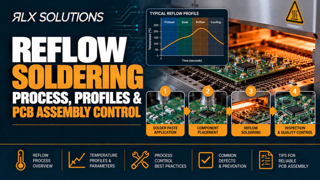
The four thermal regions of a reflow profile do different jobs
A reflow profile is the measured temperature of the assembly over time as it
travels through the oven. The important temperature is the board and component
temperature, not simply the air temperature displayed for an oven zone.
Most profiles can be understood through four functional regions.
| Profile region | Main purpose | What poor control can cause |
|---|---|---|
| Preheat | Raise assembly temperature at a controlled rate | Thermal stress, paste spatter, excessive flux loss |
| Soak | Reduce temperature differences and prepare the flux system | Premature flux exhaustion or poor thermal equalization |
| Reflow | Bring the solder above liquidus and form the joint |
Poor wetting, insufficient reflow, component damage or excessive intermetallic growth |
| Cooling | Solidify the solder joint after reflow | Uncontrolled joint structure or added thermal stress |
The exact profile cannot be selected from the solder alloy alone. Board thickness,
copper distribution, component mass, package limits, solder paste chemistry,
surface finish and oven capability all affect the result.
Preheat controls the rate of thermal change
The first problem is not simply reaching a high enough temperature. It is getting
the assembly there without creating an excessive temperature gradient.
A small passive may heat rapidly. A shield can, large connector or heavy copper
region may lag behind. If heating is too aggressive, the board and its components
experience different expansion rates. Paste can also react poorly to rapid solvent
evaporation.
A more gradual rise gives the assembly time to absorb heat while limiting the
temperature difference between fast-heating and slow-heating locations.
Soak is about thermal equalization and flux behaviour
The soak region gives colder areas of the circuit board time to catch up before
solder reaches its liquid state. It also affects flux activation.
Longer is not automatically safer. Holding the assembly hot for too long may
consume flux activity before the solder reaches the point where strong wetting is
required.
The profile therefore has to balance two competing needs: reducing board-wide
temperature variation without exhausting the chemistry that supports soldering.
Reflow has both a temperature requirement and a time requirement
Once the solder alloy passes its liquidus temperature, the paste becomes molten
and the joint forms.
A profile that barely crosses liquidus may fail to provide enough thermal exposure
for reliable wetting at the coldest location. A profile with excessive peak
temperature or excessive time above liquidus can stress components, accelerate
intermetallic growth and increase oxidation.
A useful profile therefore has a process window rather than a single magic
temperature.
For example, imagine a hypothetical lead-free assembly profiled with two
thermocouples. TC1 on a small passive reaches a 241°C peak, while TC2 beside a
thermally heavy connector reaches only 222°C. Looking only at TC1 would make
the run appear comfortably hot. The 19°C difference shows why the cold
location must also be characterized.
Cooling remains part of the soldering process
Once the assembly leaves the hottest oven zones, molten solder has to solidify.
Cooling affects solder joint microstructure and thermal stress. It also determines
how quickly downstream handling can begin safely. The process is therefore not
finished at peak temperature.
Profile the assembly, not the oven recipe
Oven zone settings are machine inputs. A thermal profile is evidence of what the
assembly actually experienced.
That difference becomes significant on boards with uneven thermal mass. Two
printed circuit boards can pass through the same oven recipe and produce
materially different component temperatures.
Profile development normally places thermocouples at locations selected to
represent meaningful thermal extremes. Useful positions include:
- A small, fast-heating component.
- A large or thermally massive package.
- A location connected to a broad copper area.
- A region close to a board edge.
- A location expected to be thermally shielded.
- A package whose temperature limit needs close observation.
Attaching every thermocouple to an easy pad near the centre of the PCB defeats
much of the purpose. The measurement plan should challenge the recipe.
The engineering question is not, “What are the oven zones set to?” It is,
“What did the hottest and coldest relevant parts of this assembly experience?”
Board A and Board B show why the same layer count can require different reflow control
Layer count alone does not describe the thermal load presented to a reflow oven.
Consider two hypothetical eight-layer assemblies.
| Decision factor | Board A | Board B |
|---|---|---|
| Layer count | 8 | 8 |
| Board thickness | 1.6 mm | 1.6 mm |
| Smallest featured package | 0.5 mm pitch QFN | 0.5 mm pitch QFN |
| Copper distribution | Moderate, relatively even | Large internal and external copper areas |
| Large components | Few | Large connector and shielded power section |
| Hidden solder joints | QFN thermal pad | QFN thermal pad plus BGA |
| Thermal behaviour | More uniform | Larger hot-to-cold temperature spread expected |
| Inspection burden | SPI, AOI, targeted X-ray | SPI, AOI, broader X-ray attention |
Both boards have eight layers and the same nominal thickness, but Board B can take
more engineering effort to profile.
Its large copper regions conduct heat away from local solder joints. The connector
body and shielded section add thermal mass. The BGA adds solder joints that
automated optical inspection (AOI) cannot directly see.
That changes cost without changing the layer count. Board B can require more
profiling work, more thermocouple placement thought and more X-ray inspection
coverage before the process window is demonstrated.
This is why assembly pricing cannot be derived reliably from layer count or
component count alone.
Thermal mass creates the profile problem engineers need to anticipate
Copper is an efficient heat conductor. That is valuable electrically and thermally
in operation, but it changes how a circuit board responds inside the oven.
A pad connected to a substantial ground or power structure can transfer heat into
the surrounding copper faster than an isolated signal pad. Large components add
another heat sink. Small packages, meanwhile, can heat much faster.
The resulting temperature difference across the PCB is often more important than
the temperature at a single measurement point.
Take a hypothetical 2.0 mm thick, six-layer board with a QFN near the centre and
a large power connector beside a wide copper region. Assume the QFN location peaks
at 239°C while the connector-side joint reaches 226°C. Increasing oven heat
may improve the cold location, but it also drives the QFN hotter.
The better response may involve changing zone balance, conveyor speed, soak
behaviour or a combination of those variables. The objective is to bring both
locations inside a usable process window rather than maximizing peak temperature
everywhere.
This same mechanism explains why copying an established profile from a visually
similar board can fail. Copper architecture that is invisible from the assembled
top view can materially change the thermal response.
Fine-pitch packages make paste control inseparable from reflow control
As lead pitch and pad geometry shrink, the acceptable margin around solder paste
deposition becomes smaller.
A 0.3 mm pitch ball grid array (BGA), an 01005 passive and a large through-hole
connector may all appear on the same mixed-technology assembly, but their process
sensitivities are different. Reflow settings have to respect the thermal
requirements of the whole assembly while stencil design and printing control the
amount of solder presented to each surface-mount joint.
This is where SPI becomes especially valuable. Catching insufficient, excessive
or displaced paste before reflow prevents the oven from converting a printing
problem into a finished solder defect.
For packages with bottom-side terminations, the control chain continues after
reflow. A BGA joint is hidden beneath the package. A QFN centre thermal pad is also
difficult to assess by surface appearance alone.
Automated X-ray inspection (AXI) allows those joints and thermal pads to be
evaluated for conditions that AOI cannot see directly, including void distribution
and hidden connection quality.
The practical sequence is therefore connected: stencil design influences deposit
geometry, SPI verifies the print, reflow forms the joint, and AXI checks hidden
outcomes.
Surface finish changes the soldering interface
Reflow does not join solder directly to bare PCB laminate. It joins the component
termination to a prepared pad surface, and that surface finish affects
solderability, planarity and process behaviour.
Common printed circuit board finishes include hot air solder levelling (HASL),
electroless nickel immersion gold (ENIG), electroless nickel electroless palladium
immersion gold (ENEPIG), immersion silver, immersion tin and organic solderability
preservative (OSP).
Finish selection should therefore happen with assembly in mind.
Planarity becomes more significant as component pitch decreases. Storage history
and surface condition also matter because the soldering process depends on
wettable surfaces. A thermally correct profile cannot fully compensate for a
compromised soldering interface.
The engineer specifying the bare board and the engineer responsible for assembly
should not treat those choices as separate systems. Reflow is where decisions from
both stages meet.
Moisture-sensitive components need control before heating
Some electronic packages absorb moisture during exposure to ambient conditions.
Reflow raises the package temperature quickly, which can turn trapped moisture
into internal vapour pressure.
The resulting damage mechanism is different from a poor solder joint, but it
occurs during the same thermal process.
Moisture-sensitive device handling therefore belongs beside profile control.
Storage, exposure history and dry handling need to be managed before the
components enter the oven.
Electrostatic discharge (ESD) control is similarly upstream. An assembly can
emerge from reflow with visually acceptable solder joints while containing a
component damaged by improper handling before placement.
Good reflow control does not replace ESD and moisture-sensitive device controls.
It assumes those controls are already working.
Inspection separates solder appearance from assembly evidence
A solder joint that looks acceptable from one viewing angle does not prove the
assembly process is under control.
Different inspection methods answer different questions:
-
SPI before reflow:
Was the intended amount of solder paste deposited in the intended position? -
AOI after reflow:
Are visible components and solder joints present, aligned and visually acceptable? -
AXI:
What happened underneath packages such as BGA, land grid array (LGA) and QFN devices? -
Manual visual inspection:
Does workmanship meet the specified IPC-A-610 Class 2 or Class 3 criteria? -
Electrical test:
Does the assembled circuit connect and operate as intended?
Inspection depth also changes with the build requirement. IPC-A-610 Class 3 calls
for tighter workmanship expectations than Class 2, so the required class needs to
be identified before the manufacturing plan is finalized.
The failure mode here is contractual as much as technical. If the build class,
inspection requirements or test expectations are left ambiguous until finished
assemblies exist, there may be no agreed basis for release.
First article approval should freeze a demonstrated process, not just approve one board
A first article inspection (FAI) is most useful when it connects the physical
assembly to the process used to manufacture it.
That means the accepted first article should correspond to controlled production
information such as the bill of materials, pick-and-place data, assembly drawing,
stencil configuration and approved process settings.
Suppose a hypothetical 12-layer board has a 0.4 mm pitch BGA, two QFNs and a dense
passive field. The first article passes SPI, post-reflow AOI and X-ray inspection,
and the functional test passes. If a later lot uses a materially different stencil
or reflow recipe without controlled review, the first article no longer represents
the same manufacturing condition.
The purpose of FAI is therefore broader than finding a cosmetically good board. It
establishes a reference point before the production lot is released.
Control changes deliberately when defects appear
Reflow troubleshooting works best when the defect is traced back to the stage
capable of creating it.
| Observed problem | First process areas to investigate |
|---|---|
| Bridging | Paste volume, stencil aperture, print alignment, placement, reflow behaviour |
| Opens | Paste deposition, component coplanarity, placement, wetting, thermal exposure |
| Tombstoning | Pad balance, paste symmetry, placement and local heating difference |
| BGA concern | Print, placement, thermal profile and X-ray evidence |
| QFN thermal-pad voiding | Paste pattern, deposited volume, package geometry and reflow behaviour |
| Repeated cold joints in one region | Local thermal mass and actual measured profile |
| Random visible defects |
Print repeatability, placement stability and process control before changing the recipe |
The table identifies starting points, not automatic diagnoses. Several mechanisms
can create a similar visual result.
The useful discipline is to change one meaningful variable with evidence behind
it. Repeatedly raising peak temperature without checking paste deposition or local
board temperature can hide the cause while shrinking the thermal margin available
to other components.
Give the assembler enough data to control reflow before production
Manufacturing control improves when the assembly package makes intent explicit.
For a PCB assembly build, the manufacturing package should include the bill of
materials, pick-and-place or centroid data, assembly drawing and the fabrication
information needed for the bare PCB. Stackup and impedance information also belong
with the fabrication package when applicable.
Beyond the basic files, flag requirements that affect the assembly process. These
can include the required workmanship class, critical component handling needs,
test requirements, programming requirements and any areas where thermal or
inspection behaviour deserves special attention.
A dense BGA field next to a large power section should not be discovered only
after the first profile run. Neither should a customer requirement for functional
test or serial traceability.
An engineer-reviewed design for manufacturability (DFM) and design for assembly
(DFA) review is the point to identify those process interactions before production
material is committed.
Reflow control is a system, not a temperature setting
The most transferable rule is to resist treating the oven recipe as the whole
soldering process.
Paste deposition determines how much solder enters the joint. Placement determines
where the terminations meet the paste. Board construction and component mass
determine how heat moves through the assembly. The thermal profile determines how
that solder and flux experience heat. Inspection then shows whether the process
produced the intended result.
A process can therefore fail even while the oven itself is operating exactly as
programmed.
For engineers, the useful questions are concrete: Where are the hot and cold
locations? Which joints are hidden? What does SPI show before reflow? Which
component or copper region drives the thermal load? What evidence releases the
first article?
Those questions produce a controllable assembly process.
Put reflow requirements into the build package before quoting
If your board is moving from prototype into controlled production, RLX reviews
assembly requirements as part of every quote. Send the Gerbers or other accepted
manufacturing files, BOM, pick-and-place data and assembly drawing so profiling,
inspection, testing and first-article requirements can be considered together
rather than after the build starts.
Reflow Soldering FAQ
What information does an assembler need to develop a reflow process?
The assembler needs the PCB manufacturing data, bill of materials, pick-and-place
data and assembly drawing, along with any requirements that affect workmanship,
testing or component handling. Thermal behaviour also depends on the physical
board and component population, so the actual assembly configuration matters
more than an isolated oven temperature target.
Why is SPI performed before reflow?
Solder paste inspection checks paste volume, area and offset before parts are
soldered. That matters because many downstream defects begin during stencil
printing. If a pad receives too much, too little or misplaced paste, changing
the reflow temperature does not necessarily correct the underlying problem.
Detecting the condition before placement and reflow prevents unnecessary defect
creation.
Why do BGA and QFN packages need X-ray inspection?
Their important solder connections are partly or completely hidden beneath the
package. Automated optical inspection can assess visible placement and solder
features, but it cannot directly view every concealed joint. X-ray inspection
provides additional evidence for BGA, LGA and QFN assemblies, including
evaluation of hidden connections and voiding beneath thermal pads.
Does every PCB use the same reflow profile?
No. The measured profile depends on the complete assembly, including board
thickness, copper distribution, component mass, package construction, solder
paste system and surface finish. Two circuit boards with similar dimensions can
respond differently if one contains heavy copper areas or thermally massive
components. Profile development therefore needs measurements from the assembly
being manufactured.
What is the difference between IPC-A-610 Class 2 and Class 3 in assembly?
Both classes define workmanship expectations for electronic assemblies, but
Class 3 applies tighter acceptance requirements than Class 2. The required class
affects how solder joints, placement and workmanship are assessed. It should be
identified before manufacturing so inspection and documentation can be planned
around the intended acceptance level rather than decided after boards are
assembled.
How is a new assembly approved before the production lot runs?
A first article provides an early manufactured unit that can be inspected and
tested before production release. Relevant checks can include solder paste
inspection, post-reflow AOI, X-ray for hidden joints, manual workmanship
inspection and electrical or functional testing where specified. Approval ties
the physical result to the manufacturing data and process used to build it.