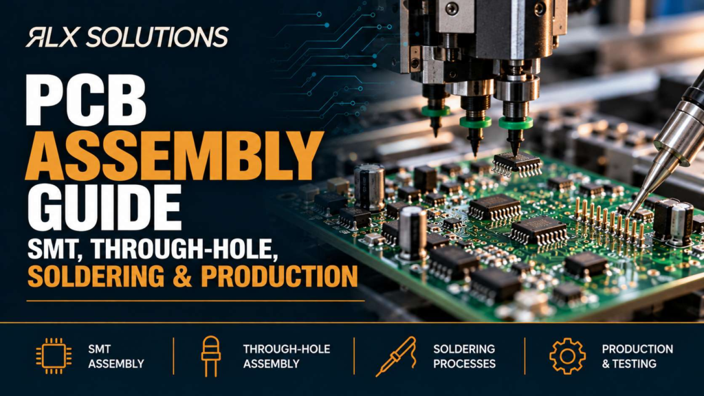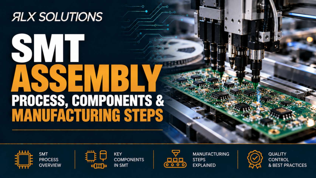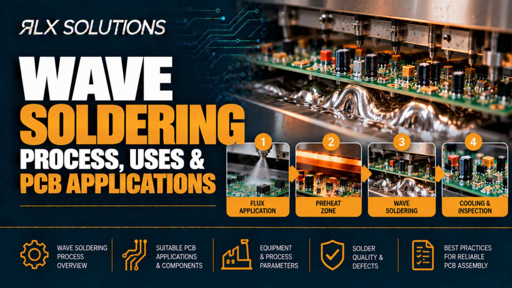
Wave soldering joins multiple through-hole component leads to a printed circuit board in one controlled pass over molten solder. RLX Solutions, a contract electronics manufacturer in Concord, Ontario, evaluates assembly method alongside board design because component mix, thermal mass, underside clearance and solder-joint requirements can change the practical process before production begins.
How wave soldering works on a PCB
Wave soldering is a bulk soldering process in which the underside of an assembled circuit board passes across a controlled wave of molten solder. Exposed component leads, plated through-holes and solderable pads contact the wave while solder mask protects areas that should remain unsoldered. For the full picture, see our PCB Assembly Guide.
The process is closely associated with through-hole technology because dozens or hundreds of leads can be soldered during the same conveyor pass. It can also be used on some mixed-technology boards after surface-mount components have already been placed and reflow soldered.
The basic mechanism is wetting. Molten solder must displace surface oxides, contact clean metal surfaces and form a metallurgical bond with the component termination and plated hole. Flux helps remove oxides and promotes wetting, while preheat prepares the assembly for the thermal transition into the solder wave.
A successful joint therefore depends on more than solder temperature. Flux application, preheat, conveyor speed, board orientation, hole geometry, component lead condition and copper distribution can all change how the joint forms.
The process is a controlled thermal and chemical sequence
Wave soldering works as a connected sequence. A problem at one stage often appears as a defect several stages later.
- Components are inserted. Through-hole leads pass through the finished plated holes. Lead diameter, hole size and component seating affect how solder can move through the barrel.
- Flux is applied. Flux conditions the exposed metal surfaces so solder can wet them. Too little can leave oxidation behind. Poorly controlled application can also produce inconsistent results across the same board.
- The assembly is preheated. Preheat raises board and component temperature before solder contact. It activates the flux and reduces the thermal shock created when a relatively cool assembly reaches molten solder.
- The PCB meets the solder wave. The conveyor brings the underside into controlled contact with the wave. Solder enters the annular area around the lead and moves into the plated through-hole through wetting and capillary action.
- The joint separates from the wave. Separation behaviour matters. Excess solder must drain without creating bridges between neighbouring pads or leaving elongated solder projections.
- The assembly cools. The solder solidifies into the final joint. Inspection and electrical testing then determine whether the assembly meets the specified acceptance requirements.
This sequence explains why changing one design variable can force a process adjustment. A large connector tied into several copper planes extracts more heat than an isolated signal pin. Running both through the same thermal profile without accounting for that difference can produce acceptable joints in one area and marginal joints in another.
Worked example: two connectors on the same board
Consider a 1.6 mm thick, 6-layer PCB.
Connector X has 20 signal pins, each using a 0.8 mm lead in a 1.1 mm finished hole. Most pins connect to narrow traces.
Connector Y has four 1.0 mm power leads in 1.3 mm holes, with each lead tied into large internal copper areas on multiple layers.
Both components enter the same solder wave. Their thermal behaviour is different.
Connector X reaches soldering temperature relatively quickly because each joint is connected to limited copper. Connector Y transfers heat away from its joints through the planes. If the profile is chosen around Connector X alone, the power connections may wet more slowly or show weaker barrel fill.
The problem is not simply large holes versus small holes. It is the complete thermal path from solder, through the pin and plated barrel, into the copper structure of the PCB.
Where wave soldering fits best
Wave soldering is most attractive when the board contains enough conventional through-hole joints to justify processing many of them together.
Typical applications include connectors, headers, switches, relays, transformers, large capacitors and other components whose leads pass through the circuit board. Through-hole attachment may be selected for mechanical retention, package availability, electrical requirements or component form factor.
The economic advantage comes from parallel processing. A row of 40 connector pins can cross the solder wave in the same production pass instead of being soldered individually.
That advantage becomes smaller when only a handful of through-hole joints remain. A board with four isolated pins may not benefit from the same production method as one with 300 accessible through-hole connections.
Board geometry matters as well. Tall hardware, bottom-side surface-mount devices, closely packed connectors and heat-sensitive parts may interfere with wave access or make shielding necessary.
Mixed-technology boards change the soldering decision
A mixed-technology PCB combines surface-mount technology (SMT) and through-hole components on the same assembly. These boards commonly use more than one soldering process.
One possible manufacturing sequence is:
- Apply solder paste to the SMT side.
- Place surface-mount components.
- Reflow the SMT joints.
- Insert through-hole components.
- Solder the remaining through-hole joints using wave or another controlled process.
- Inspect and electrically test the completed assembly.
The difficulty is underside exposure. During wave soldering, the bottom surface approaches the solder. Any component, pad or feature placed there must be compatible with that process or physically protected from it.
Some bottom-side SMT parts can be designed into a wave process, often with attention to component orientation, spacing and retention. Others make a full-board solder wave unattractive.
This is where assembly planning should happen during layout rather than after boards have been fabricated.
A placement decision that appears harmless in computer-aided design can dictate additional masking, custom tooling or a different soldering method on the production floor.
Wave soldering vs selective soldering vs hand soldering
Wave, selective and manual soldering can all create through-hole joints, but they solve different manufacturing problems.
| Decision factor | Wave soldering | Selective soldering | Hand soldering |
|---|---|---|---|
| Processing approach | Large underside area passes over solder wave | Solder is applied to targeted locations | Operator solders individual joints |
| Best fit | Many accessible through-hole joints | Through-hole joints surrounded by sensitive or inaccessible features | Low joint count, rework or special situations |
| Board exposure | Broad | Localized | Highly localized |
| Throughput potential | High when joint count is large | Focused processing without exposing the full underside | Limited by individual joint processing |
| Mixed-technology flexibility | Depends heavily on underside layout | Better isolation around nearby SMT features | Flexible but labour intensive |
| Key design concern | Wave access and board orientation | Nozzle access and keep-out space | Operator access and repeatability |
Selective soldering is localized through-hole soldering. Instead of presenting much of the underside to a broad solder wave, the machine brings controlled solder contact to selected joints or groups of joints.
That distinction becomes valuable on dense mixed-technology assemblies.
Suppose a board has 180 through-hole joints distributed across eight large connectors with an open underside. A wave process can address the group efficiently.
Now suppose another board has only 16 through-hole pins positioned between ball grid array (BGA), land grid array (LGA) and quad flat no-lead (QFN) components already mounted nearby. Full underside exposure creates a different process problem. Localized soldering may reduce the number of features that must be protected.
Hand soldering remains useful when access, quantity or rework requirements make automated processing unnecessary, but relying on manual soldering for a high pin count changes labour content and increases the importance of operator consistency.
Why two 6-layer boards can have very different soldering costs
Layer count alone does not describe assembly difficulty. Two boards can have identical layer counts while demanding different soldering processes, tooling and inspection effort.
Board A vs Board B
Both hypothetical boards are 6-layer, 1.6 mm thick designs.
| Factor | Board A | Board B |
|---|---|---|
| Through-hole joints | 220 | 220 |
| Main connectors | Four 2.54 mm pitch headers | Four 2.54 mm pitch headers |
| Bottom-side SMT near connectors | None within 8 mm | Multiple parts within 1.5 mm |
| Power-plane connections | Limited | Several connector pins tied to large planes |
| Solder access | Open underside | Restricted by nearby SMT |
| Likely process challenge | Thermal profile and bridge control | Localized access, protection and thermal variation |
Board A gives the soldering process an open working area. Its primary challenges are controlling wetting, thermal balance and solder separation across many pins.
Board B has the same layer count and the same number of connector joints, but the underside layout adds constraints. Nearby SMT components may force masking, specialised tooling or a localized soldering strategy. Large plane-connected pins also create greater thermal demand.
The assembly cost difference therefore comes from process conditions, not from the fact that both boards have six copper layers.
This is one reason an assembly quotation cannot be inferred reliably from board dimensions and component count alone.
Design details decide whether solder can form a repeatable joint
Wave soldering rewards layouts that give solder a predictable path to the joint and away from it.
Hole and lead geometry
The component lead must physically fit the plated hole while leaving enough space for insertion and solder flow. A hole that is unnecessarily tight can complicate insertion and restrict solder movement. A very loose fit changes solder volume and component positioning.
Consider a hypothetical connector using a 0.9 mm square lead. Designing around a finished hole without checking the lead’s maximum diagonal dimension can create an insertion problem even if the nominal numbers appear close.
Finished hole size, plating and component tolerances should therefore be evaluated together.
Pad spacing and solder bridging
Closely spaced through-hole pads create a smaller physical separation for molten solder to clear as the board leaves the wave. Orientation relative to conveyor travel can affect how solder drains from rows of pins.
A 2.00 mm pitch connector presents a different bridge-control problem from a 5.08 mm pitch terminal block. The tighter pitch gives the process less separation between adjacent solderable features.
Copper distribution and thermal mass
Copper removes heat from the joint.
A ground pin connected directly to a large internal plane behaves differently from a signal pin connected to a narrow trace, even when both leads and holes have identical dimensions.
Thermal relief patterns can reduce heat transfer from plated holes into large copper areas. Their use must still satisfy the electrical and current requirements of the design.
Solder mask
Solder mask defines protected areas around solderable features. Dam geometry, pad openings and registration affect how effectively neighbouring features remain separated.
Mask design becomes more significant as pad spacing decreases. A layout that removes mask between adjacent pads changes the physical barrier available to resist solder bridging.
Surface condition
Solderability is the ability of a metal surface to be wetted by molten solder and form an acceptable joint. Surface finish, oxidation, contamination, handling and storage history can all affect it.
Bare PCB finishes such as hot air solder levelling (HASL), electroless nickel immersion gold (ENIG), immersion silver, immersion tin and organic solderability preservative (OSP) protect exposed copper in different ways. The assembly process should be developed with the actual board finish and material condition in mind.
Common wave soldering defects point back to specific mechanisms
A defect is more useful when treated as evidence of a process condition rather than as an isolated visual problem.
Solder bridges form when solder remains connected between adjacent conductors after the board leaves the wave. Pitch, pad geometry, board orientation, solder drainage and process settings can all contribute.
Insufficient solder or incomplete barrel fill can appear when wetting is poor or the joint does not receive enough usable thermal energy. Plane-connected pins often deserve added attention because the surrounding copper conducts heat away.
Open joints occur when the required electrical and metallurgical connection fails to form. Contaminated surfaces, oxidation, poor flux activation or inadequate solder contact can contribute.
Solder balls are small detached solder particles left on the board. Flux behaviour, mask condition and process settings are among the factors that can affect their formation.
Icicles or projections appear when solder stretches away from a joint and freezes before it can retract. Separation dynamics and temperature behaviour are part of the mechanism.
The useful production question is therefore not just whether a defect exists. It is whether the defect pattern follows a connector, a board region, a copper condition or the direction of travel through the process.
That pattern often reveals where the manufacturing cause sits.
Inspection and test continue after soldering
Wave soldering ends when the joint solidifies, but assembly acceptance does not.
Visual inspection checks joint formation, bridging, component seating, polarity and other workmanship conditions. IPC-A-610 defines acceptability criteria for electronic assemblies, with Class 3 applying tighter workmanship expectations than Class 2.
J-STD-001 addresses soldered electrical and electronic assemblies from the process and workmanship side. The two standards are related but should not be treated as interchangeable.
Electrical testing asks a different question. A joint can look acceptable but still sit in a circuit with an open net, incorrect component, polarity error or other assembly fault.
Testing may therefore include in-circuit approaches, flying probe testing, fixture-based testing or functional test depending on product design and production stage. X-ray is particularly useful for hidden solder joints such as BGA, LGA and QFN connections elsewhere on a mixed-technology assembly, even though those packages are generally associated with reflow rather than the wave itself.
For a new assembly, first article inspection adds another control point before the remaining production quantity is released.
Prepare the assembly package around the real soldering constraints
If your PCB combines through-hole connectors, surface-mount components and thermally heavy copper features, the soldering route should be reviewed before production files are released. RLX includes engineer-reviewed design for manufacturability and design for assembly review with every quote, so Gerbers, bill of materials, centroid data and assembly drawings can be assessed as one manufacturing package.
FAQ
Can surface-mount components go through wave soldering?
Some mixed-technology designs allow selected bottom-side surface-mount components to pass through a wave process, but package geometry, orientation, spacing and retention all matter. Many assemblies instead reflow the SMT components first and then use wave or selective soldering for through-hole parts. The correct sequence should be decided from the actual underside layout rather than from component type alone.
Is wave soldering still used for modern circuit boards?
Yes. It remains relevant where a PCB contains enough through-hole connections for group processing to make sense. Connectors, terminal blocks, relays and other leaded components can create substantial through-hole joint counts even on assemblies dominated by SMT. Dense mixed-technology layouts may shift some of those joints toward selective soldering instead.
What is the difference between reflow and wave soldering?
Reflow soldering normally starts with solder paste printed onto surface-mount pads. Components are placed into the paste, and the assembly is heated so the solder melts and forms joints. Wave soldering normally brings the underside of an assembly into contact with molten solder, making it particularly useful for through-hole joints and selected compatible bottom-side features.
Why do large ground pins sometimes solder differently from signal pins?
Large ground or power connections can conduct heat from the plated hole into copper planes. That increases the thermal load at the joint. A signal pin attached to a narrow trace may reach soldering temperature more easily. Hole geometry can be identical while the two joints behave differently because their internal copper connections are different.
When does selective soldering make more sense than wave soldering?
Selective soldering becomes attractive when only certain through-hole areas should contact molten solder. Dense bottom-side SMT, restricted access or widely separated connector groups can make broad wave exposure inconvenient. A board with hundreds of accessible through-hole pins may still favour wave processing, while one with a few isolated connectors may benefit from localized soldering.
What files help a manufacturer evaluate the soldering process?
The useful package normally includes fabrication data, drill information, assembly drawings, a bill of materials and pick-and-place or centroid data. Stackup information and clear assembly notes also help the manufacturer understand board construction, component location and thermal conditions. The goal is to evaluate the bare PCB and assembled circuit board as one production system rather than as separate files.