
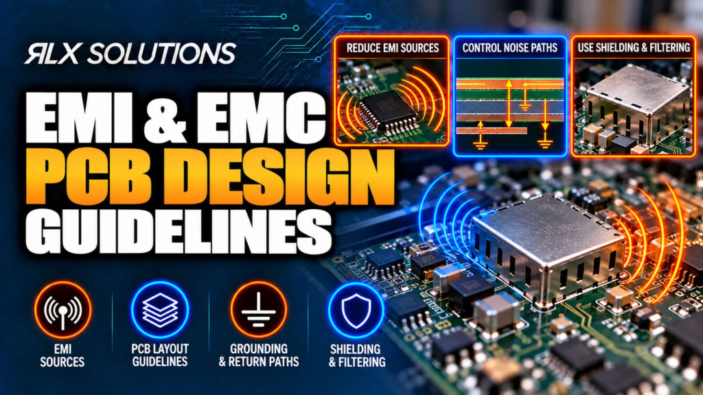
Electromagnetic interference (EMI) is controlled most effectively in the PCB layout, not after a compliance failure. Good electromagnetic compatibility (EMC) design keeps high-frequency current loops small, gives signals continuous return paths, controls switching fields and prevents cables from becoming unintended antennas. RLX Solutions, a contract electronics manufacturer in Concord, Ontario, reviews these interactions as part of PCB design work.
The useful distinction is simple. EMI is unwanted electromagnetic energy generated by or coupled into a circuit. EMC is the ability of the complete product to operate acceptably in its electromagnetic environment without creating unacceptable interference.
A board can therefore function perfectly on the bench and still have an EMC problem. The schematic may be electrically correct while the physical implementation creates large current loops, return-path discontinuities, noisy connector currents or excessive coupling between switching and sensitive circuits.
Start EMI Control With Current Loops, Not Trace Length
The most useful PCB design question is not simply, “Is this trace short?” Ask where the signal current goes and where its return current flows.
Every signal forms a current loop. At higher frequencies, return current tends to remain close to the signal conductor because that path reduces loop inductance. A trace routed over a continuous reference plane therefore has a compact electromagnetic field structure.
Interrupt that plane and the situation changes.
Suppose a clock travels 35 mm across Layer 1 with a solid Layer 2 ground reference. Its return current can remain close beneath the trace. Now cut a 12 mm slot in Layer 2 and route the same clock across it. The return current must find another path around the discontinuity. The resulting loop becomes larger, which increases the opportunity for radiation and coupling.
That is why “short traces” is incomplete EMI advice. A slightly longer trace over an uninterrupted reference plane can be preferable to a shorter trace that crosses a plane split.
Treat the signal conductor and its return conductor as one routing structure.
Build the Stackup Around Field Containment
Layer count alone does not determine EMC performance. The relationship between signal layers and their reference planes matters more.
For a multilayer printed circuit board, critical signals should have an adjacent, continuous reference plane wherever practical. That plane provides the high-frequency return path and helps contain the electromagnetic field associated with the trace.
A useful planning sequence is:
- Identify clocks, fast digital interfaces, switch-node regions and sensitive analogue circuits.
- Decide which reference plane each critical routing layer will use.
- Determine how return current will transfer when a signal changes layers.
- Establish controlled-impedance requirements before final routing.
- Check whether power distribution, routing density and reference-plane continuity justify additional layers.
This work belongs at stackup definition, not at the end of PCB layout.
Consider a hypothetical 6-layer board:
| Layer | Function |
|---|---|
| Layer 1 | Components and critical signals |
| Layer 2 | Ground reference |
| Layer 3 | Signals / power routing |
| Layer 4 | Power / signals |
| Layer 5 | Ground reference |
| Layer 6 | Components and signals |
A Layer 1 clock can reference Layer 2. A Layer 6 high-speed interface can reference Layer 5. But a transition from one routing layer to another still requires you to consider how the return current moves between reference structures.
A signal via solves the signal conductor’s vertical transition. It does not automatically solve the return current’s transition.
Preserve Return Paths Through Layer Changes
A high-speed signal changing layers can create an EMI problem even when the trace geometry on both layers looks correct.
If both routing layers reference ground planes, nearby ground stitching vias can provide a short return-current transition between those planes. Without that path, return current may travel farther through the board before finding an interplane connection.
For a differential pair, the same principle applies. Differential signalling can reduce external field coupling because the two conductors carry opposing currents, but real differential pairs are never perfectly balanced. Reference-plane continuity still matters.
Do not use “differential” as permission to ignore the return structure.
This becomes particularly important around dense ball grid arrays (BGAs), where fanout, layer transitions and reference changes can occur within a small area. Via-in-pad can help dense routing by placing a filled, capped and planarized via within a component pad. When that structure is used, its fabrication requirements need to be established with the stackup rather than added after routing is complete.
Keep Ground Planes Continuous Unless the Circuit Requires Otherwise
Splitting ground is sometimes presented as a universal way to separate noisy digital circuitry from sensitive analogue circuitry. Physical separation of functional blocks can be valuable. Arbitrarily cutting the reference plane beneath their signals can create a different problem.
A high-frequency signal crossing a split loses the direct return path beneath the trace. Return current then travels around the split or through another available connection, enlarging the current loop.
A better starting point for many mixed-signal layouts is:
- Keep the ground reference continuous.
- Separate noisy and sensitive circuits through placement.
- Keep switching currents confined to their intended regions.
- Route signals so their return currents do not pass through sensitive areas.
- Control where analogue and digital functions interact.
The distinction matters. Functional partitioning separates current paths intentionally. A plane slot can force current paths apart unintentionally.
If isolation requirements demand separate electrical domains, the layout needs to be designed around that isolation architecture from the beginning. That is different from cutting a ground plane as a general noise-control technique.
Decoupling Is a Loop-Inductance Problem
A decoupling capacitor is useful only if high-frequency current can move through the capacitor, device power pin and return path with sufficiently low impedance.
That makes placement and connection geometry important.
Imagine a processor with a decoupling capacitor 3 mm from its power pin. The capacitor connects to power and ground using short connections and nearby vias. Compare that with the same nominal capacitor 25 mm away, connected through narrow traces.
The capacitance printed on the component is unchanged. The high-frequency current path is not. Extra conductor length adds parasitic inductance, reducing the capacitor’s effectiveness as frequency rises.
For PCB layout, focus on the complete loop:
power pin → capacitor → ground/reference structure → device ground → internal switching circuit
Keep that loop compact.
Bulk capacitance elsewhere on the board serves a different frequency range and current-delivery function. It does not substitute for local high-frequency decoupling.
Control Switching-Regulator Hot Loops at the Source
Switch-mode power supplies deserve special treatment because they combine high current with rapid voltage and current transitions.
The highest-risk region is usually the switching loop carrying rapidly changing current. Large loop area increases magnetic-field radiation. A large switch-node copper area can increase electric-field coupling.
Keep the relevant input capacitor and switching devices close enough to minimize the high di/dt loop. Keep the switch-node area no larger than required for electrical and thermal performance. Do not route sensitive analogue signals through or beneath a noisy switching region without considering coupling through the stackup.
Filter placement also matters. A filter positioned after noise has already coupled into a large PCB region may have less effect than one positioned at the boundary between the noisy circuit and the rest of the system.
Route Fast Signals by Edge Rate, Not Just Clock Frequency
A 10 MHz digital signal is not necessarily a “10 MHz layout problem.”
Digital edges contain frequency components far above the fundamental repetition rate. A low-frequency clock with fast rise and fall times can therefore create transmission-line and EMI behaviour that would be missed if you classified nets only by clock frequency.
High-speed interfaces such as PCI Express (PCIe), USB 3.x, HDMI, Ethernet, SerDes and DDR memory require control of impedance, reference continuity, transitions and coupling. A controlled-impedance trace is a transmission structure whose geometry and surrounding dielectric establish its characteristic impedance.
For controlled-impedance PCB fabrication, the stackup cannot be an afterthought. Trace width, copper thickness, dielectric spacing and material properties interact. Fabrication also changes the final geometry from the idealized values in the layout database.
Board A vs Board B: Same Layer Count, Different EMC Risk
Two boards can have the same layer count, dimensions and component count yet create very different fabrication and EMC outcomes.
Consider two hypothetical 8-layer designs.
| Decision Factor | Board A | Board B |
|---|---|---|
| Layer count | 8 | 8 |
| Critical signal reference | Continuous adjacent ground | Several reference interruptions |
| BGA fanout | Through vias | Layer 1 to Layer 2 microvias plus buried-via structure |
| Fast-signal layer changes | Limited | Frequent |
| Switching regulator | Compact hot loop | Wider switching loop |
| Connector routing | Filtered near boundary | Fast traces cross board before filtering |
| Return-path planning | Defined with stackup | Addressed after routing |
Board A is electrically simpler even though both boards contain eight layers. Board B adds sequential fabrication considerations through its blind or buried structures while also making the electromagnetic design harder through frequent reference transitions.
The pricing difference would therefore not be explained by layer count alone. Board B can require additional fabrication stages and tighter coordination between stackup, via architecture and routing.
More important for EMC, its layout creates more locations where return-current continuity must be managed.
Keep Noisy and Sensitive Functions Apart by Placement
Component placement determines where current flows before a trace is drawn.
A practical board floorplan should identify at least four types of regions:
- High di/dt power switching.
- Fast digital logic and clocks.
- Sensitive analogue or measurement circuitry.
- External interfaces and connectors.
Putting a high-gain analogue input beside a switching node creates a coupling problem that may be difficult to solve with routing. Moving the analogue input farther away changes both capacitive and magnetic coupling before additional filtering is considered.
Likewise, placing an external connector beside the noise source can allow filtering close to the board boundary. Placing the connector on the opposite side may force noisy currents across a large portion of the circuit board.
Treat Connectors and Cables as Part of the EMC Design
A PCB can have low local radiation while still failing radiated-emissions testing because noise reaches an attached cable.
Common-mode current is particularly important here. It is current flowing in the same direction on multiple conductors relative to another reference, rather than equal and opposite currents confined within the intended signal circuit.
Review every off-board interface for:
- The signal’s intended return path.
- Common-mode conversion.
- Connector ground arrangement.
- Filtering location.
- Shield termination where applicable.
- High-frequency current paths through protection components.
- Routing between the interface circuit and connector.
Put interface filtering where it controls current at the boundary. A filter connected through long traces may introduce enough parasitic inductance to weaken its high-frequency performance.
Electrostatic discharge (ESD) protection deserves the same geometric thinking. The discharge current needs a deliberate path that does not carry the transient through sensitive circuitry before reaching its intended return.
Via Fences Help Only When They Complete a Real Current Path
Ground stitching vias are useful around board edges, RF regions, layer transitions and shielding structures, but adding more vias indiscriminately is not an EMC strategy.
Near a high-speed signal transition, stitching vias can help return current move between reference planes. Along a grounded perimeter, multiple connections can reduce the inductance between copper structures. Around an RF region, they can contribute to field containment when used as part of a designed ground structure.
A row of vias cannot repair a signal routed across an inappropriate plane split or compensate for a poorly placed switching converter.
Surface Finish Does Not Fix an EMI Layout
Surface finish affects exposed copper surfaces, solderability and assembly considerations. It is not a substitute for return-path control, grounding or field containment.
Changing from one suitable surface finish to another does not repair a clock crossing a reference-plane slot.
Assembly quality also matters for the final hardware. Incorrect component placement, solder defects or unexpected behaviour beneath bottom-terminated components can alter circuit operation and complicate debugging. Inspection methods such as solder paste inspection (SPI), automated optical inspection (AOI) and X-ray inspection address assembly quality, while electrical and functional testing determine whether the assembled hardware behaves as specified.
Design for the Compliance Test Before Layout Release
EMC testing should not be the first point at which the team decides what electromagnetic behaviour the product needs.
The target market and product category determine which regulatory requirements apply. Those requirements can include conducted emissions, radiated emissions and immunity tests. The PCB designer needs those system-level requirements early enough to influence stackup, connector architecture, filtering, shielding provisions and board placement inside the enclosure.
Before releasing the design, review:
- Every high-frequency signal and its return path.
- Reference-plane continuity through layer changes.
- Clock and fast-edge routing.
- Switch-mode power loops.
- Local decoupling geometry.
- External connector current paths.
- Interface filtering.
- Analogue and digital partitioning.
- Unused or accidental antenna structures.
- Controlled-impedance requirements.
- Shielding and chassis connections, where applicable.
- Fabrication details that could change the intended geometry.
Give the Manufacturer the Electrical Intent, Not Just Gerbers
Gerbers describe PCB geometry. They do not communicate every electrical assumption behind that geometry.
For an EMI-sensitive design, the manufacturing package should make stackup and controlled-impedance intent explicit. Manufacturing files can include Gerber RS-274X, ODB++, IPC-2581 data and NC drill files, supported by a stackup document, impedance targets and fabrication notes where required.
Suppose a hypothetical 10-layer, 1.6 mm board contains a 100-ohm differential interface on Layer 3 referenced to Layer 2. If the designer communicates only nominal trace width and spacing, the manufacturer sees geometry. If the package also identifies the impedance target and intended stackup, fabrication engineering can treat those dimensions as part of an electrical structure.
If the same 10-layer board uses 0.10 mm laser-drilled microvias from Layer 1 to Layer 2 and Layer 2 to Layer 3 to escape a dense BGA, the via architecture also becomes part of stackup planning. Stacked or staggered microvias, filled and capped structures, and via-in-pad construction affect the manufacturing sequence.
Electrical, mechanical and fabrication decisions converge in the same few millimetres of PCB.
Review EMI and EMC Before the First Board Is Built
The cheapest EMC problem to correct is the one identified while the board still exists as design data.
An effective design review should follow current paths rather than inspect nets in isolation. Start at each noise source, follow its signal and return path, inspect every layer transition, then follow potential coupling paths toward connectors, cables and sensitive circuitry.
For a board containing DDR memory, USB 3.x, Ethernet and a switching power stage, that review crosses signal integrity, power delivery, stackup, component placement and EMI/EMC concerns. Those disciplines interact physically on the same printed circuit board.
If you are preparing a design for fabrication or assembly, RLX can review PCB layout, stackup, impedance, power delivery and EMI/EMC considerations before release, with engineer-reviewed DFM included as part of the quote process.
Frequently Asked Questions
What is the difference between EMI and EMC in PCB design?
EMI is unwanted electromagnetic energy that a circuit generates or receives. EMC describes whether the complete product can operate correctly in its electromagnetic environment without creating unacceptable interference. PCB design affects both because stackup, return paths, switching loops, connectors and filtering determine how electromagnetic energy is generated, coupled and conducted through the product.
Can a two-layer PCB have good EMC performance?
A two-layer PCB can be appropriate for some designs, but limited layer count makes continuous reference structures and power distribution harder to maintain as routing density and edge rates increase. The decision should be based on current-return paths, circuit complexity and EMC requirements rather than assuming a particular layer count guarantees a pass or failure.
Do differential pairs still need a ground reference?
Yes. Differential signalling reduces reliance on a reference plane compared with a single-ended signal because much of the intended current is exchanged between the pair. Real routing still has imbalance, discontinuities and common-mode energy, so reference continuity remains important. Layer transitions, connector transitions and pair asymmetry deserve particular attention during an EMC review.
Should analogue and digital grounds always be separated?
No. Physical separation of noisy and sensitive functions can be useful, but cutting a ground plane can interrupt signal return paths. The grounding architecture should follow the circuit’s current paths and isolation requirements. For many mixed-signal designs, careful placement and routing over a continuous low-impedance reference avoids problems created by signals crossing ground-plane splits.
Does controlled impedance improve EMC?
Controlled impedance can support EMC performance because it creates predictable transmission structures and helps reduce reflections and field discontinuities on fast signals. It does not guarantee compliance by itself. Reference continuity, return-current transitions, connector design, decoupling and common-mode current still need to be controlled across the complete board and system.
What files are useful for an EMI-aware PCB design review?
The useful package depends on the review stage. Design work can use native files from Altium, Eagle, KiCad, OrCAD or DipTrace. Manufacturing release can include Gerber RS-274X, ODB++, IPC-2581 and NC drill data, plus stackup documentation, impedance targets and fabrication notes. Assembly packages additionally need the BOM, pick-and-place data and assembly drawing.


Pingback: PCB Shielding: EMI Control Methods | RLX Solutions