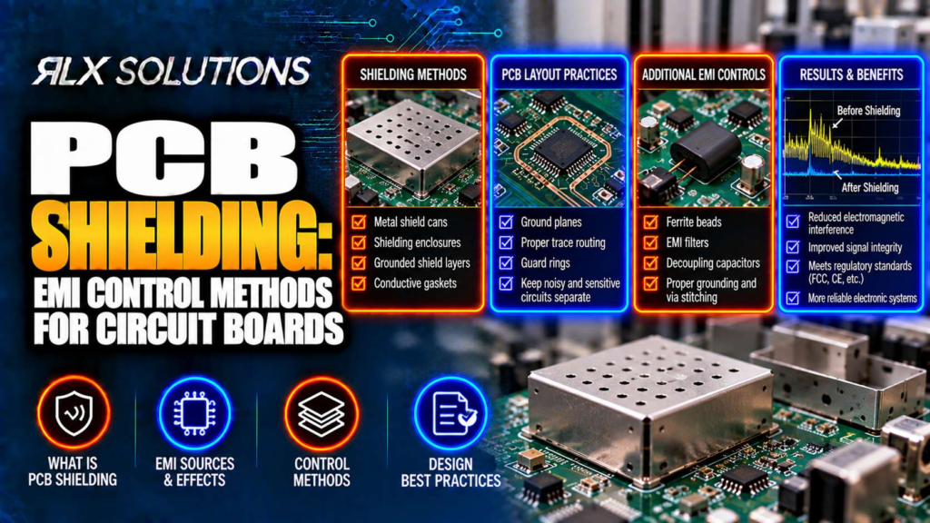
PCB shielding works best when it is treated as part of the electromagnetic interference (EMI) control strategy, not as a metal cover added after testing fails. RLX Solutions, a contract electronics manufacturer in Concord, Ontario, reviews shielding alongside stackup, grounding, routing, filtering and enclosure decisions because each method addresses a different coupling path.
Start With the EMI Coupling Path, Not the Shield
A shield can reduce radiated coupling, but it cannot correct every EMI problem on a printed circuit board. Before adding metal, identify three things: the noise source, the coupling path and the susceptible circuit. For the full picture, see our PCB Engineering Guide.
Conducted interference travels through copper, cables, power rails or shared impedance. Radiated interference couples through electric or magnetic fields. Near-field coupling can also occur between traces, planes, inductors, connectors and other structures before energy ever reaches the enclosure.
That distinction changes the remedy.
| EMI mechanism | PCB control method | Why it works |
|---|---|---|
| Electric-field coupling | Ground planes, spacing, shielding | Reduces capacitive coupling and intercepts field energy |
| Magnetic-field coupling | Smaller current loops, placement, return-path control | Reduces loop area and magnetic flux coupling |
| Common-impedance coupling | Power and ground architecture | Reduces voltage developed across shared impedance |
| Conducted noise | Filtering and controlled return paths | Attenuates unwanted current before it reaches an interface |
| Radiated emissions | Routing, reference planes, shielding, enclosure design | Limits antenna structures and contains remaining field energy |
| Cable radiation | Connector grounding, filtering, common-mode control | Prevents the cable from becoming the dominant antenna |
This is why a board can still fail electromagnetic compatibility (EMC) testing inside an apparently substantial shield. If noise is leaving through a cable, crossing a split reference plane or coupling through shared impedance, the shield may be addressing the wrong path.
The cost consequence appears late. A shield added after layout can consume component clearance, require mounting features, interfere with thermal paths and force enclosure changes. Finding the coupling mechanism during layout leaves more options available.
Use the PCB Stackup as the First Shielding Structure
A continuous reference plane is one of the most useful EMI-control structures available to a PCB designer. It gives high-frequency return current a low-inductance path close to the signal trace and reduces the loop area formed by the outgoing and returning currents.
Loop area matters because every current loop can behave as an antenna. Increasing the separation between a signal and its return path increases the field produced by that loop. A stackup that keeps high-speed signals close to a reference plane therefore addresses emissions before an external shield is considered.
Consider a hypothetical 6-layer, 1.6 mm circuit board:
- Layer 1: high-speed signals and components
- Layer 2: solid ground reference
- Layer 3: lower-speed signals
- Layer 4: power distribution
- Layer 5: solid ground reference
- Layer 6: signals
A clock routed on Layer 1 directly over Layer 2 has a nearby return path. If the same signal changes layers through a via and continues on Layer 6 referenced to Layer 5, the return current also needs a practical transition between those reference structures. Ignoring that transition can create a larger current loop exactly where the signal changes layers.
The via is therefore not just a geometric connection between signal layers. From an EMI perspective, the designer must also account for how the electromagnetic field and return current move through the stackup.
This becomes especially important around board edges, connectors and reference-plane discontinuities. Copper should not be treated as an abstract zero-impedance node. At high frequencies, geometry controls current flow.
Keep High-Frequency Return Paths Continuous
A fast signal crossing a reference discontinuity can create more EMI than its trace length suggests.
Return current follows the path of lowest impedance. At high frequency, that usually means remaining close to the signal conductor. A split, slot or poorly planned plane transition forces the return current away from that preferred path. The resulting loop grows, increasing inductance and potentially increasing radiation and coupling into nearby structures.
This problem often appears when mixed-signal partitioning is interpreted as a reason to cut ground planes. Functional separation on the schematic does not automatically mean that a physical slot belongs under a high-speed trace.
The same reasoning applies to board edges. A high-frequency trace placed close to the edge can couple energy into surrounding structures more readily than one located over a continuous internal reference with appropriate edge clearance.
PCB fabrication also imposes physical limits on the proposed geometry. Copper-to-edge spacing, trace width, spacing and the selected stackup need to be evaluated together rather than after routing has been completed.
Via Fences Turn Ground Copper Into a Better RF Boundary
Ground stitching vias connect ground structures through the board. A via fence is a repeated line of those connections, commonly placed near board edges, RF regions or boundaries where field containment matters.
The mechanism is important. Ground copper on Layer 1 and Layer 6 does not automatically behave as one continuous high-frequency structure simply because both nets are named GND. The vias provide physical connections between those conductive surfaces.
Spacing is frequency-dependent. A fence that behaves effectively at one frequency may be too sparse at a substantially higher frequency, so there is no universal via pitch that solves every shielding problem.
Worked Example: The Same 8-Layer Board, Two Different EMI Strategies
Assume two hypothetical 8-layer boards have the same outline, thickness and digital circuitry.
| Decision factor | Board A | Board B |
|---|---|---|
| Layer count | 8 | 8 |
| Sensitive RF region | Ground pour nearby | Ground pour plus via-fenced boundary |
| High-speed layer change | Signal via only | Signal transition planned with nearby ground return |
| Shield provision | None | Footprint reserved for a board-level shield |
| Connector region | General ground connection | Connector return path treated as part of EMI design |
| Manufacturing effect | Fewer EMI-specific features | More drills, copper features and shield-related assembly requirements |
Board B is not automatically the better design. If Board A already meets emissions and immunity requirements, the additional structures may provide no product-level benefit.
The important difference is that Board B creates several deliberate field and return-current controls. Its via fence, transition strategy and shield footprint also consume routing area and manufacturing features. Two boards with the same layer count can therefore have different fabrication and assembly costs because layer count alone does not describe their electromagnetic architecture.
Board-Level Shields Work Only With a Good Ground Connection
A board-level shield is a conductive barrier placed around an EMI source, a susceptible circuit or both. It can reduce electric-field coupling and, depending on frequency, geometry and material, can contribute to magnetic-field attenuation.
The shield is only one part of the structure. Its connection to the PCB matters.
A shield with a long, inductive path to ground can perform very differently from one connected around its perimeter through short conductive paths. At high frequencies, a connection that looks perfectly adequate on a DC schematic can have enough inductance to undermine shielding performance.
Shield openings also matter. Seams, ventilation holes, cable exits and large gaps can allow electromagnetic energy to couple through the barrier. The relevant dimension is not simply the percentage of open area. Opening geometry relative to wavelength and field distribution matters.
Board-level shielding generally falls into several practical forms:
- One-piece soldered cans. Useful when the shield does not need to be removed during normal servicing.
- Frame-and-lid systems. A soldered frame remains on the PCB while the lid can be removed for access.
- Partitioned shields. Internal walls isolate multiple regions within one shielded area.
- Enclosure-level shielding. The product enclosure becomes part of the electromagnetic boundary rather than placing a can around an individual circuit.
The mechanical design needs to be considered during PCB layout. A shield footprint competes with traces, vias, components and test access. The assembly process also needs sufficient clearance for placement, inspection and rework.
Control EMI at Connectors Before the Cable Becomes an Antenna
A shielded PCB can still radiate through an attached cable.
Common-mode current on an interface cable is particularly troublesome because even a relatively small unwanted current can turn a long cable into an efficient radiator. The connector boundary is therefore one of the first places to examine when emissions appear to be associated with an external interface.
Filtering is most effective when unwanted energy is diverted or attenuated before it spreads across the board or enters the cable. Component selection alone is insufficient. Placement and return geometry determine whether the filter works as intended at high frequency.
Suppose a hypothetical 4-layer board carries a high-speed interface from a processor to a connector 70 mm away. Moving the filtering components from 45 mm inside the board to immediately adjacent to the connector changes more than placement convenience. The second arrangement shortens the unfiltered path between the filter and the external interface.
The same reasoning applies to connector shields. If a cable shield is intended to intercept high-frequency current, the connection between the cable shield and the product’s shielding structure needs low high-frequency impedance. A long trace wandering through the digital ground system can defeat the intended current path.
Cable assemblies can also require programme-specific shielding and electrical tests. Board and cable shielding should therefore be treated as one interface problem rather than two unrelated drawings.
Separate Sensitive and Noisy Circuits by Current Path
Placement is an EMI-control method.
Switching power stages, clocks and fast digital interfaces can generate substantial high-frequency energy. High-impedance analogue nodes, RF receivers and precision measurement circuits may be susceptible to much smaller disturbances. Increasing physical separation helps, but separation works best when current paths are also controlled.
For a switching regulator, inspect the high di/dt loops rather than treating the entire regulator circuit as equally noisy. Keeping those loops physically small reduces magnetic-field generation. Positioning sensitive traces away from the switching node reduces capacitive coupling.
A shield placed over a poor power layout may suppress some radiated field without fixing the source mechanism. A smaller switching loop can reduce the field before shielding becomes necessary.
The same principle affects layer assignment. A sensitive trace on an internal layer between reference structures can have a different coupling environment from a trace routed on an exposed outer layer. Moving a trace without understanding its reference plane, however, can simply trade one problem for another.
Shielding and Controlled Impedance Must Be Designed Together
High-speed signal integrity and EMI are closely connected because both depend on electromagnetic fields and return paths.
Controlled impedance sets a target relationship among conductor geometry, dielectric properties and reference structures. Changing trace width, dielectric thickness or reference-plane geometry to solve an EMI issue can therefore change impedance.
That creates a common design trap. Late placement of shielding pads, stitching vias or ground features can consume routing space and force high-speed traces into geometries that differ from the intended impedance structure.
For controlled-impedance circuit boards, the stackup should be resolved before the final routing geometry is frozen. Time-domain reflectometry (TDR) on a fabrication coupon can then verify the manufactured impedance against the specified target.
The manufacturer needs more than a generic note saying “controlled impedance.” The fabrication package should identify the impedance target and stackup information needed to resolve the physical construction.
HDI Can Improve Routing Freedom, but It Changes the Build
High-density interconnect (HDI) techniques can help when EMI constraints compete with dense component escape routing.
A microvia is a laser-drilled interconnection used to connect selected layers over a short vertical distance. Blind vias connect an outer layer to one or more inner layers without passing through the complete PCB. Buried vias connect internal layers without reaching either outer surface.
These structures can free routing space and allow designers to manage transitions around dense ball grid arrays (BGAs). They also change fabrication.
For example, imagine a 10-layer board with a 0.5 mm pitch BGA. Board A escapes the package using through vias wherever routing permits. Board B uses Layer 1 to Layer 2 microvias and internal buried connections so that through-hole barrels do not consume routing channels across every layer.
Board B may gain routing freedom, but the build sequence is more involved. Blind vias on multilayer stackups require sequential lamination, while filled and capped via-in-pad structures add filling, planarization and copper-cap operations. The EMI benefit must therefore come from a real routing or return-path improvement, not from using HDI by default.
Aspect ratio also remains part of the fabrication decision for drilled structures. Hole diameter and board thickness cannot be chosen independently when reliable plating is required.
Surface Finish Does Not Replace EMI Design
Surface finish affects solderability, assembly and exposed copper protection. It should not be selected as a substitute for an electromagnetic shielding strategy.
The distinction matters because shield frames, removable lids, grounding contacts and connector structures can create assembly requirements that interact with finish selection. A design that expects soldered shielding hardware has different manufacturing considerations from one that relies on enclosure contacts.
Finish also needs to match the broader assembly process. Shielding hardware should therefore be included when the board’s finish and assembly flow are selected.
If the product uses edge contacts, wire bonding or another specialised interconnect, that requirement may drive the finish decision independently of EMI. The electromagnetic architecture and the assembly architecture still need to coexist on the same physical board.
Plan Inspection and Test Around the Shield
Shielding can hide the very solder joints and components that need inspection.
That matters with BGAs, land grid arrays (LGAs), quad flat no-lead (QFN) packages and other connections where X-ray inspection may be part of the assembly plan. A shield installed too early can obstruct inspection, rework or probing.
The assembly sequence should therefore answer several questions before the shield footprint is released:
- Which components require automated optical inspection (AOI) after reflow?
- Which hidden joints require X-ray inspection?
- Does in-circuit or functional testing require probe access inside the shielded region?
- Is firmware programming performed before or after shield installation?
- Can a failed component be reworked without destroying the shield structure?
- Does the first article need inspection before the shield is permanently attached?
The contractual consequence is straightforward. If the shield changes test access, that information belongs in the manufacturing package and assembly planning. Leaving it to the production floor creates unnecessary interpretation at the point where changes are most expensive.
Give the Manufacturer the EMI-Critical Information
Gerbers alone describe copper geometry, but they do not always communicate the design intent behind EMI-critical structures.
For a bare PCB, the manufacturing package can include Gerber RS-274X, ODB++ or IPC-2581 data with NC drill information. Stackup documentation and impedance targets are also relevant when controlled structures are involved.
For an assembled printed circuit board, the bill of materials (BOM), pick-and-place or centroid data and assembly drawing establish the additional production information.
For EMI-sensitive designs, make the intended structures unambiguous. Identify shield footprints and hardware, controlled-impedance requirements, stackup, critical ground features and assembly constraints rather than expecting the manufacturer to infer why a copper feature exists.
This is particularly important when a late fabrication adjustment could alter an electromagnetic boundary. A seemingly minor change to copper, drilling or assembly clearance can have a functional consequence if the feature is part of the return-current or shielding structure.
Design Shielding Before EMC Testing Forces a Redesign
The lowest-risk EMI strategy is layered. Reduce noise at the source, control current loops, maintain return paths, filter external interfaces and then use shielding where field containment is still required.
That order also preserves engineering options. Once the board outline, connector locations, enclosure and assembly sequence are fixed, the available fixes become increasingly mechanical and expensive.
A useful design review should therefore connect several disciplines that are often handled separately:
- Map likely high-frequency noise sources and sensitive circuits.
- Review reference planes and return-current continuity.
- Check high-speed layer transitions.
- Examine switching-current loops and connector interfaces.
- Decide where ground stitching or via fencing serves a defined electromagnetic purpose.
- Reserve shield footprints and mechanical clearance where containment may be required.
- Confirm that impedance, drilling and stackup remain manufacturable.
- Preserve inspection, programming, test and rework access.
The result is not necessarily a board with more shielding. It is a board where every shielding feature has a specific coupling mechanism to address.
Move EMI Decisions Into the Manufacturing Review
If you are preparing an EMI-sensitive circuit board for prototype or production, RLX can review the fabrication and assembly package as part of the engineer-reviewed design for manufacturability (DFM) process. Send the manufacturing files, stackup documentation, impedance targets and applicable assembly data so electromagnetic design decisions can be checked against the proposed physical build.
Frequently Asked Questions
Does every PCB need an EMI shield?
No. Many boards can control EMI through placement, stackup, continuous reference planes, routing, filtering and return-path design without a board-level shield. A shield is most useful when it addresses an identified field-coupling problem or isolates a specific noisy or sensitive region. Adding one without identifying the coupling mechanism can increase cost and assembly constraints without solving the failure.
Can a ground plane replace a shielding can?
They perform different functions. A nearby reference plane controls return-current geometry and reduces loop area, while a shielding can creates a conductive boundary around a region. A strong plane structure may reduce the need for additional shielding, but it does not automatically provide the same containment as an enclosure around a radiating or susceptible circuit.
Do stitching vias reduce EMI?
They can when they create a useful high-frequency connection between ground structures or help form a boundary around a region. Their effectiveness depends on geometry, frequency and the electromagnetic path being controlled. Adding arbitrary ground vias is not equivalent to designing a via fence around a specific field-containment or return-current requirement.
Should an EMI shield be installed before or after circuit testing?
The sequence should preserve the inspection and test access required by the assembly. AOI, X-ray inspection, in-circuit test, functional test, programming and rework may all affect when a shield can be installed. Shield hardware and its installation stage should therefore be identified during assembly planning rather than decided after production begins.
What PCB files are needed for an EMI-sensitive design?
Bare-board manufacturing can use Gerber RS-274X, ODB++, IPC-2581 and NC drill data, with stackup documentation and impedance targets where applicable. Assembly additionally requires the BOM, pick-and-place or centroid file and assembly drawing. EMI-critical shield footprints, grounding structures and assembly restrictions should be clearly represented rather than left for manufacturing interpretation.
Can controlled impedance and EMI requirements conflict?
They can interact because both depend on conductor geometry, dielectric construction and reference planes. Adding ground features, changing layer relationships or rerouting around shield hardware can alter an impedance-controlled structure. Resolve the stackup, impedance requirements and EMI architecture together before finalising high-speed routing so a late shielding change does not create a new signal-integrity problem.