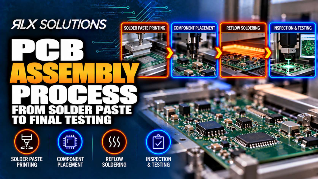
The PCB assembly process turns a fabricated circuit board into a tested electronic assembly through controlled printing, placement, soldering, inspection and verification. RLX Solutions, a contract electronics manufacturer in Concord, Ontario, follows this sequence because defects become harder and more expensive to diagnose once the board moves beyond the process step that created them.
A bare PCB has already completed fabrication before assembly begins. Assembly adds components and creates the electrical and mechanical connections required by the design. Surface-mount technology (SMT), through-hole assembly or a mixed-technology process may be used depending on the component set.
The important point is that assembly is not simply a placement operation followed by a final inspection. Each stage creates evidence about the stage before it. Solder paste inspection can expose printing problems before components are placed. Automated optical inspection can expose placement and solder-joint defects after reflow. X-ray inspection reaches joints hidden beneath packages. Electrical and functional tests then determine whether the completed hardware behaves as intended.
Assembly Starts Before Solder Paste Reaches the Board
A repeatable PCB assembly process starts with manufacturing data, material control and first-article preparation. The assembler needs enough information to know what gets installed, where it goes, how the finished assembly should look and how it will be tested.
A typical manufacturing package includes:
- BOM: The bill of materials identifies the specified components.
- Pick-and-place or centroid data: Defines component coordinates, rotation and placement references.
- Assembly drawing: Communicates component orientation and assembly-specific instructions.
- Bare-board manufacturing data: Gerber RS-274X, ODB++ or IPC-2581 data may support the underlying printed circuit board build.
- Test requirements: Define what must be electrically or functionally verified after assembly.
The BOM deserves particular attention. A correct reference designator paired with the wrong manufacturer part number can produce an assembly that looks perfect under automated optical inspection (AOI) but is electrically wrong.
Material handling matters as well. Moisture-sensitive devices require controlled storage and handling because absorbed moisture can become vapour during reflow. Electrostatic discharge controls protect sensitive components before there is any visible evidence of damage.
Component sourcing adds another risk layer. Authorized distribution provides a direct supply path, while obsolete, allocated or otherwise difficult parts may require additional verification. Packaging inspection, date-code and country-of-origin checks, visual inspection, lot verification, X-ray or electrical testing can become part of the incoming process when authenticity risk warrants it.
Before a new build proceeds into its production lot, first article inspection (FAI) provides a controlled point to verify the assembly against the released manufacturing data.
Step 1: Solder Paste Printing Controls the Joint Before Reflow
For SMT assembly, solder paste is deposited onto exposed pads through a stencil. Paste contains metal solder particles suspended in flux and other materials that allow it to print, hold components and form solder joints during reflow.
Printing sounds simple, but small variations have downstream effects. Too little paste can produce insufficient solder. Too much can contribute to bridging or excessive solder. Poor registration can place paste off-centre from the pad.
Solder paste inspection (SPI) measures paste volume, area and offset before reflow. Inspecting 100% of assemblies at this point creates an early process gate. A printing problem can be corrected before placement and heating convert it into a solder-joint problem.
Consider a hypothetical board carrying a 0.5 mm pitch device. A small paste-position error may still leave material on every pad, so a simple presence check can miss the problem. Measuring offset shows whether the deposited paste is centred sufficiently for the subsequent placement and reflow stages.
That distinction matters economically. Rejecting or correcting a paste print happens before the board has accumulated the full cost of placement, reflow, inspection and test.
Step 2: Component Placement Turns CAD Data Into Physical Hardware
Once paste deposition is accepted, pick-and-place equipment positions surface-mount components onto their assigned pads.
The centroid file tells the equipment where components belong and how they are oriented. The BOM identifies what each reference designator should contain. The assembly drawing supplies another human-readable reference for orientation and build requirements. These data sets have to agree.
A rotation error illustrates the problem. Imagine a 6-layer circuit board with a 0.5 mm pitch integrated circuit at U12. The BOM can identify the correct part and the placement file can contain the correct X-Y coordinate, yet an incorrect rotation value can still put Pin 1 in the wrong orientation. Placement accuracy alone cannot rescue incorrect manufacturing data.
Package geometry also changes the process challenge. Assembly can extend from larger passive components to very small packages such as 01005 passives and fine-pitch ball grid arrays (BGAs). As features shrink, paste deposition, placement, pad design and inspection become increasingly interconnected.
A BGA presents a different inspection problem from a gull-wing package because its solder joints sit underneath the component body. That difference affects the inspection strategy after reflow, not just placement.
Step 3: Reflow Creates the Surface-Mount Solder Joints
After placement, the populated board passes through a reflow process. Heat activates the flux and brings the solder alloy through the thermal conditions required to wet the component terminations and PCB pads. Cooling then solidifies the joints.
The mechanism is thermal, but the result is mechanical and electrical.
A component that looked correctly positioned before reflow can move as molten solder and surface tension act on it. Paste volume differences can contribute to uneven joints. Package and pad geometry can create soldering conditions that are difficult to evaluate from the top surface alone.
This is why the PCB assembly process cannot treat reflow as a final quality gate. Reflow converts the deposited paste into joints, but those joints still have to be inspected.
Surface finish on the bare PCB also enters the assembly equation because the assembler is soldering to the finish applied during fabrication. Options such as electroless nickel immersion gold (ENIG), hot air solder levelling (HASL), electroless nickel electroless palladium immersion gold (ENEPIG), immersion silver, immersion tin and organic solderability preservative (OSP) create different fabrication and assembly considerations.
The board finish is therefore not an isolated fabrication decision. It reaches directly into solderability, process planning and the number or type of thermal exposures the board is expected to experience.
Step 4: Post-Reflow Inspection Separates Visible and Hidden Defects
Post-reflow inspection asks a different question from SPI. SPI evaluates the printed paste before components are soldered. AOI evaluates the assembled board after reflow.
AOI can inspect both sides of the assembly. It is useful for detecting visible conditions such as component presence, position, orientation and accessible solder-joint characteristics.
But optical inspection has a physical limit: a camera cannot directly inspect a joint hidden beneath an opaque package.
That is where automated X-ray inspection (AXI) becomes important. X-ray can inspect packages and structures such as:
- BGA solder joints
- Land grid arrays (LGAs)
- Quad flat no-lead (QFN) packages
- Thermal-pad solder regions
- Solder voiding
A 0.3 mm Pitch BGA Changes the Inspection Problem
Take a hypothetical board with a 0.3 mm pitch BGA. The package body hides its ball connections after placement and reflow. AOI can still evaluate visible features around the device, but it cannot see through the package to judge every hidden solder connection.
X-ray addresses that geometry by creating an image from material-density differences through the assembly. This allows the inspection process to look beneath the component instead of trying to infer hidden-joint quality solely from external appearance.
That distinction is important for design for assembly. Package selection determines more than placement difficulty. It can determine which inspection method is capable of seeing the joint at all.
Manual visual inspection under magnification remains another part of the process. Workmanship requirements may be applied to IPC-A-610 Class 2 or Class 3 builds, with Class 3 imposing tighter workmanship expectations.
Step 5: Through-Hole and Mixed-Technology Boards Add Another Soldering Sequence
Not every component can or should pass through the same SMT process. Connectors, large components and other devices may use plated through-holes instead.
A mixed-technology board combines SMT and through-hole components, so the assembly route has to account for both.
Selective soldering is one way to solder targeted through-hole locations without exposing every part of an already assembled board to the same soldering operation. The exact sequence matters because the board may already contain reflowed SMT components when through-hole parts are added.
A simple hypothetical mixed board shows the scheduling effect. Suppose an 8-layer, 1.6 mm-thick circuit board contains 0603 passives, a QFN controller and two through-hole connectors. The SMT side can proceed through paste printing, placement and reflow first. The connectors then require their own insertion and soldering operations before final inspection and test.
Adding two through-hole connectors did not add only two placement actions. It introduced another process path.
Same Layer Count Does Not Mean the Same Assembly Cost
Layer count is primarily a bare-board fabrication characteristic, but two assemblies built on boards with the same layer count can require very different assembly effort.
Consider two hypothetical 10-layer designs:
| Decision Factor | Board A | Board B |
|---|---|---|
| PCB layer count | 10 layers | 10 layers |
| Smallest common passive | 0603 | 01005 |
| Fine-pitch package | 0.8 mm pitch BGA | 0.3 mm pitch BGA |
| Through-hole content | None | Two connectors |
| Hidden joints | BGA | Fine-pitch BGA plus QFN thermal pad |
| Primary assembly route | SMT | SMT plus through-hole |
| Inspection implication | SPI, AOI, X-ray where required | SPI, AOI and greater dependence on X-ray |
| Additional process implication | Standard SMT sequence | Additional insertion and soldering sequence |
Board B introduces smaller components, tighter package geometry, more hidden solder joints and a second assembly technology. Those differences affect handling, process control and inspection even though both printed circuit boards have exactly ten layers.
This is why assembly quotations need the BOM, centroid data and assembly drawing rather than layer count alone. The assembler has to see the component and process conditions that actually drive the build.
Step 6: Electrical Test Finds Faults Inspection Cannot See
Inspection and electrical test answer different questions.
An optical or X-ray system examines physical assembly conditions. Electrical test checks whether the circuit connections behave as expected. A solder joint can look acceptable yet still participate in an electrical fault elsewhere in the network.
In-circuit test (ICT) can be approached differently depending on build conditions.
Flying-probe ICT does not require a dedicated bed-of-nails fixture, making it useful for prototype and lower-volume work. Probes move between test points to check circuit nets.
Bed-of-nails ICT uses a fixture with physical probes positioned for the particular board. The fixture adds preparation, but the fixed probing arrangement suits production testing where repeated access to the same nodes is required.
Testability therefore begins during PCB layout.
If important nodes are inaccessible, the electrical test strategy loses options. Test-point planning is a design-for-test decision, not something that can always be solved after the first production boards have been assembled.
For example, suppose two versions of a controller expose the same signals electrically. Version A provides accessible test points on power rails and key digital nets. Version B routes the same nets beneath dense packages without accessible probe locations. The schematic function may be identical, but the physical test strategy is not.
Step 7: Functional Testing Checks What the Finished Assembly Actually Does
Functional test (FCT) moves beyond individual nets and asks whether the assembled board performs according to the customer’s test specification.
That may involve powering the board, stimulating inputs, observing outputs or executing a defined pass/fail sequence. Results can be logged with serial traceability when the program requires it.
This distinction between ICT and FCT matters.
ICT is valuable for locating assembly-level electrical problems such as connectivity faults. Functional testing evaluates behaviour closer to the board’s intended operation. One does not automatically replace the other because they expose different failure classes.
Firmware may also be part of this stage. In-system programming can use interfaces such as ISP/ICSP, JTAG or SWD for bootloader and firmware flashing. Serialization can associate the physical assembly with identifiers such as serial markings or programmed MAC addresses.
Once programming becomes part of manufacturing, configuration control becomes part of assembly control. Loading the wrong firmware revision can produce a board with excellent solder joints that still fails its intended function.
Step 8: Final Release Depends on Evidence Collected Throughout the Build
Final testing should confirm the outcome of a controlled process, not serve as the first serious attempt to discover whether assembly succeeded.
By the time a board reaches release, evidence may have accumulated from several stages:
- Incoming component and material controls
- Solder paste inspection
- Placement and reflow
- Automated optical inspection
- X-ray where package geometry requires it
- Manual workmanship inspection
- In-circuit testing
- Functional testing
- Programming and serialization where specified
- First article approval for a new build
This layered approach improves fault isolation. If SPI passes but post-reflow AOI repeatedly identifies the same solder condition, the investigation can focus on what changed after printing. If physical inspection passes but FCT fails, attention can move toward electrical behaviour, component correctness, programming or design-level causes.
Traceability makes that evidence useful beyond one board. Process documentation, component lot and date codes, and test records can connect a finished assembly back to the material and manufacturing history behind it.
Class 2 and Class 3 Change the Acceptance Context
IPC-A-610 governs electronic assembly workmanship, and Class 2 and Class 3 represent different performance expectations. Class 3 applies tighter workmanship requirements than Class 2.
The practical implication is that class selection reaches into inspection, documentation and acceptance criteria. It should be defined before production rather than added as an informal requirement after boards have already been built.
Fabrication and assembly requirements also need to remain distinct. IPC-6012 applies to rigid printed circuit board fabrication, while IPC-A-610 addresses assembly workmanship. A Class 3 assembly requirement does not erase the need to define the corresponding bare-board requirements appropriately.
Soldering workmanship also connects with J-STD-001. These standards operate at adjacent stages of the manufacturing problem, which is why purchase documentation should state the required build and acceptance expectations clearly.
Coating, Underfill and Rework Come After the Core Assembly Decisions
Some assemblies require processes beyond soldering and electrical test.
Conformal coating can use acrylic, silicone, polyurethane or parylene and may cover selected areas or the full board. Underfill can be applied where the package and application call for additional support. Potting and encapsulation create another level of environmental or mechanical protection.
These operations have a sequencing consequence: once material covers the assembly, access changes.
That affects inspection, test and rework planning. A fault that is straightforward to access on an uncoated board can become more difficult after coating or encapsulation. Test strategy and acceptance gates therefore need to account for the point at which access becomes restricted.
BGA rework presents a similar example. Removal, reballing or replacement changes a soldered package after the original assembly operation, so verification after rework matters. X-ray can be used to inspect the resulting hidden joints.
The engineering question is not simply whether a secondary process is available. It is where that process belongs in the route so that the board has already passed the inspections and tests that become harder afterward.
Give the Assembler Enough Data to Control the Process
A clean PCB assembly process depends on released data that describes the same product consistently across design, sourcing, placement, inspection and test.
Before sending a build for quotation, check that the BOM, pick-and-place file and assembly drawing agree on reference designators and component orientation. Include the test requirements that will determine final acceptance. Where the bare board has controlled stackup or impedance requirements, include the relevant fabrication documentation as well.
If you are preparing a printed circuit board for prototype or production assembly, RLX can review the manufacturing package as part of the quotation process. Send the BOM, pick-and-place data, assembly drawing and applicable board files so the build, sourcing and test requirements can be evaluated together.
PCB Assembly Process FAQs
What files are needed for PCB assembly?
A PCB assembly package normally includes a BOM, pick-and-place or centroid file and assembly drawing. Bare-board manufacturing data may include Gerber RS-274X, ODB++ or IPC-2581 files plus NC drill data. Stackup information, impedance targets and fabrication notes should accompany the package where applicable. Test requirements also need to be communicated when electrical or functional testing is expected.
What is the difference between SPI and AOI?
Solder paste inspection checks paste before reflow, including volume, area and offset. Automated optical inspection occurs after reflow and examines the assembled board for visible placement and soldering conditions. The two methods control different stages. SPI can identify printing problems before components are soldered, while AOI evaluates the physical result after the assembly has passed through reflow.
Why are BGA components X-rayed after reflow?
A ball grid array places its solder connections underneath the component body, where normal optical inspection cannot directly see them. X-ray inspection can evaluate hidden BGA connections and is also applicable to LGA packages, QFN thermal pads and void analysis. The package geometry therefore determines why X-ray becomes part of the inspection plan.
Does every assembled PCB need functional testing?
Functional testing is performed to a customer-defined specification, so the required test strategy needs to be established for the program. FCT checks board behaviour rather than simply examining solder joints or individual connections. Where specified, pass/fail results can be logged with serial traceability, connecting the test result to the individual assembly.
What is the difference between flying-probe and bed-of-nails ICT?
Flying-probe in-circuit testing uses moving probes and does not require a dedicated fixture, which makes it useful for prototypes and lower-volume builds. Bed-of-nails ICT uses a board-specific fixture and is suited to repeated production testing. Both depend on the board providing suitable electrical access, so testability should be considered during layout rather than after assembly.
Can PCB assembly include programming and serialization?
Yes. Programming can include ISP/ICSP, JTAG or SWD interfaces as well as bootloader and firmware flashing. Serialization can include serial marking, programmed MAC addresses, laser marking or labels. These operations should be controlled alongside the assembly documentation because the correct physical hardware can still fail final acceptance if the wrong firmware or identity data is applied.