Lead free solder for PCB assembly is commonly selected where product compliance and manufacturing requirements call for a tin-silver-copper alloy such as SAC305, while Sn63Pb37 remains relevant where a tin-lead process is explicitly specified. The largest process difference is thermal: the tin-silver-copper alloy melts over about 217°C to 220°C, while eutectic Sn63Pb37 melts at 183°C, so the reflow window, component exposure, wetting behaviour and rework conditions change with the alloy.
RLX Solutions, a contract electronics manufacturer based in Concord (Vaughan), Ontario, supports SMT and through-hole assembly in SAC305 or tin-lead solder. SAC305 standard; Sn63Pb37 on request.
Lead Free Solder vs Leaded Solder in PCB Assembly
For buyers comparing lead free vs leaded solder, the choice is not a cosmetic material substitution. The alloy changes the temperature at which joints form, the way molten solder wets the pad and termination, the joint microstructure after cooling, and the thermal load placed on the PCB and components during assembly.
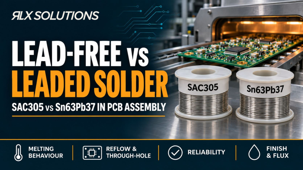
SAC305 is 96.5% tin, 3.0% silver and 0.5% copper. It has a solidus near 217°C and a liquidus near 220°C. Sn63Pb37 is 63% tin and 37% lead. It is eutectic, which means it changes from solid to liquid at a single temperature, 183°C, rather than passing through a melting range.
| Decision factor | SAC305 | Sn63Pb37 |
|---|---|---|
| Nominal composition | 96.5Sn / 3.0Ag / 0.5Cu | 63Sn / 37Pb |
| Melting behaviour | 217°C solidus to about 220°C liquidus | Eutectic at 183°C |
| Process implication | Requires a higher-temperature thermal process | Allows soldering at a lower thermal level |
| Joint behaviour | Stiffer tin-rich joint with different creep and fatigue behaviour | More ductile tin-lead joint |
| Compliance direction | Common choice where lead restriction applies | Used only where the product requirement and applicable regulation permit it |
| Process change risk | Requires profile, paste, finish and rework settings suited to the lead-free alloy | Requires a controlled tin-lead process and material segregation where both alloys are handled |
The table is useful, but it does not make the decision by itself. If the product specification requires a lead-restricted material system, the tin-silver-copper option is usually the practical direction. If a legacy design, approved drawing, regulatory exemption or other controlled requirement explicitly calls for Sn63Pb37, changing the alloy can alter a qualified process and should be treated as an engineering change.
SAC305 and Sn63Pb37 Behave Differently Under Heat
The melting-point gap is the first process difference an engineer should account for. The tin-silver-copper alloy must be heated above its liquidus so the alloy can fully melt and wet the joint surfaces. Sn63Pb37 reaches the liquid state at 183°C, giving the process a lower thermal requirement.
That difference affects more than the oven setting. A printed circuit board contains materials with different thermal mass and heat capacity. Small passives heat quickly. Large connectors, shields, copper planes and power components absorb more energy. A profile therefore has to bring the coldest relevant solder joint through the required process window without exposing the hottest component or board region to excessive heat.
Consider a hypothetical comparison. Board A and Board B are both 8-layer, 1.6 mm FR-4 assemblies with a 0.5 mm pitch QFN, a BGA and a large power connector. Board A uses the lead-free alloy. Board B uses Sn63Pb37. The layer count, board thickness and component population are identical, but Board A requires a profile that takes every required joint above the 220°C liquidus region. Board B reaches liquid solder at 183°C. The same oven recipe would therefore be a poor assumption even though the boards look identical.
The reflow soldering process guide covers profile development, thermal regions and inspection control in depth. Its focus is process profiling, while the decision here is why the solder alloy changes that profile requirement in the first place.
The tin-silver-copper alloy also has a narrow melting range rather than a single eutectic point. During heating and cooling, the alloy passes through a short region where solid and liquid phases coexist. That difference is small in temperature, but it is part of why process settings should be based on the paste supplier’s data and measured board temperatures instead of a copied recipe.
What Changes in Reflow and Through-Hole Assembly?
Changing alloy changes the thermal process, flux system and contamination controls around the soldering operation. Surface-mount technology (SMT) reflow, wave soldering, selective soldering and hand rework can all use either alloy family, but the setup should match the material system being built.
For SMT, the paste contains both alloy powder and flux. The paste supplier defines the intended thermal behaviour of that specific chemistry. A profile that works for one paste cannot be assumed to work for another merely because both pastes use the same nominal alloy. Flux activation, solvent behaviour, oxidation control and time above liquidus all interact with the alloy.
For through-hole work, the same principle applies to a solder pot. A change between tin-lead and lead-free materials is not just a bar-alloy substitution. Pot metallurgy, component termination finishes, flux, preheat and contact conditions all affect the result. The wave soldering process and PCB applications guide covers the wave process itself, including how preheat, flux and solder contact fit together.
Material segregation also matters where both alloy systems exist in the same manufacturing environment. Cross-contamination can change alloy composition and make process control harder. Tools, solder pots, hand-solder consumables and rework practices should follow the approved process for the build.
A second hypothetical example shows the assembly consequence. Imagine a 6-layer, 2.0 mm mixed-technology board with a 0.5 mm pitch QFN, forty 0402 passives and two 20-pin through-hole connectors. The SMT side may be reflowed first, followed by selective soldering for the connectors. If the product specification calls for the lead-free alloy, both operations need a compatible lead-free material system. If Sn63Pb37 is specified instead, the soldering materials and process records need to stay consistent with that requirement.
Reliability Depends on the Failure Mechanism, Not the Alloy Label
Neither alloy is universally more reliable. Reliability depends on the loading the solder joint will experience, including thermal cycling, vibration, mechanical shock, board flexure, package geometry and the coefficient-of-thermal-expansion mismatch between the component and PCB.
The tin-silver-copper alloy is tin-rich and generally stiffer than Sn63Pb37. Its microstructure contains tin-rich phases and silver-copper intermetallic compounds. Sn63Pb37 is more ductile and has a different creep response. Those differences matter because a solder joint is both an electrical connection and a mechanical interface that absorbs strain as the assembly heats, cools and flexes.
For a large ball grid array package, thermal expansion mismatch can cycle the corner joints repeatedly. For a small passive, the dominant concern may instead be pad geometry, board bending or asymmetric heating. For a heavy through-hole connector, mechanical loading through the housing and leads can matter more than the nominal alloy family.
The engineering mistake is to reduce the decision to a single claim such as “lead-free is stronger” or “leaded is more reliable.” A stronger or stiffer joint can transfer more strain into another part of the interconnect. A more ductile joint can absorb strain differently. The correct question is which failure mode the product must resist and which alloy system has been qualified for that use.
Defect control should also be separated from long-term reliability. Bridging, tombstoning, opens and voiding are manufacturing outcomes influenced by paste volume, wetting, thermal balance, stencil design, pad geometry and component placement. The guide to soldering defects in PCB assembly covers bridges, tombstones and voids as process defects rather than treating them as alloy labels.
Surface Finish, Flux and Inspection Must Match the Alloy
The solder joint forms at an interface between the solder, the component termination and the PCB pad finish. That means alloy selection cannot be separated from the bare-board finish and the flux chemistry.
Common finishes include lead-free hot air solder levelling, tin-lead HASL, electroless nickel immersion gold (ENIG), immersion silver, immersion tin and organic solderability preservative (OSP). Finish selection affects pad planarity, solderability and the metallurgical interface that forms during soldering. The PCB surface finish comparison for ENIG, HASL and OSP covers those bare-board trade-offs in detail.
Flux is equally connected to the process. Flux removes oxides and supports wetting while the joint is heated. Its activation range, residue chemistry and compatibility with the thermal profile matter. A higher-temperature alloy can place different demands on the flux system than a lower-temperature eutectic alloy.
“No-clean” also does not mean “no residue.” It describes a flux system whose residue may be acceptable to remain under the intended process conditions. Whether residue becomes a concern depends on the chemistry, amount, location, electrical spacing, product environment and any cleanliness requirement. The no-clean flux and PCB cleaning guide explains the residue decision in more detail.
Inspection should then verify the result appropriate to the package type. Solder paste inspection (SPI) checks deposition before reflow. Automated optical inspection (AOI) checks visible placement and solder features after reflow. Automated X-ray inspection (AXI) is used where joints are hidden under packages such as BGA, LGA and QFN devices. Manual visual inspection applies the specified workmanship criteria. Electrical or functional testing addresses circuit behaviour rather than joint appearance alone.
The alloy does not replace any of these controls. It changes the process conditions under which those controls have to work.
Choose the Alloy at the Product Requirement Level
The solder alloy should be set by the product requirement, not by habit at the assembly line. Start with the drawing, compliance requirement, approved material declaration, existing qualification basis and component restrictions.
A practical decision sequence is:
- Confirm the regulatory requirement. Determine whether the finished product must meet a lead-restriction regime such as RoHS and whether any applicable exemption exists.
- Check the released engineering documentation. If the drawing or approved manufacturing specification names the approved lead-free alloy or Sn63Pb37, treat that as a controlled requirement.
- Review component and PCB finish compatibility. Confirm that terminations, board finish and process materials match the intended alloy system.
- Review the thermal budget. Higher-temperature soldering affects the PCB, component packages, moisture-sensitive devices and rework conditions.
- Define the inspection and test plan. Workmanship class, hidden-joint inspection and electrical or functional test requirements should be established before production.
- Control material changes. Switching alloy, paste or flux after a process has been approved should be handled through engineering change control rather than as a shop-floor substitution.
This sequence is especially useful for legacy products. A mature assembly may have years of drawing history, component alternates and prior qualification built around one solder system. Moving to another alloy may be technically possible, but the change can affect profile settings, component exposure, finish interactions and the evidence used to approve the assembly.
Specify the Alloy Clearly in the Manufacturing Package
The assembler should not have to infer the alloy from a RoHS logo, an old BOM note or the colour of a previous solder joint. Put the requirement into the controlled manufacturing package. For how the two substance regimes differ at board level, see RoHS and REACH obligations compared for circuit boards.
For an assembled PCB, provide:
- Gerber RS-274X, ODB++ or IPC-2581 fabrication data
- NC drill data where applicable
- bill of materials in .xlsx or .csv format
- pick-and-place or centroid data
- assembly drawing
- fabrication notes
- required solder alloy or approved material specification
- required workmanship class
- test requirements
- any component-specific thermal or handling restrictions
If a product is moving from Sn63Pb37 to the lead-free alloy, flag that as a process change. The manufacturer can then review the thermal profile, surface finish, component terminations, paste system, rework method and inspection plan as one controlled package.
For Class 2 or Class 3 workmanship, the required class should also be stated before assembly. IPC-A-610 governs assembly acceptability, while J-STD-001 covers soldered electrical and electronic assemblies and process requirements. The alloy decision sits inside that broader manufacturing definition.
Send Your Files for an Assembly Quote
Gerbers, BOM, pick-and-place. An RLX engineer reads every inquiry and replies with DFM/DFA feedback and any BOM flags before your build is quoted. RLX Solutions works under an ISO 9001:2015 certified quality system. Request a quote or send your files to sales@rlxsolutions.com.
Frequently Asked Questions
Is SAC305 the same as lead-free solder?
No. This is one specific lead-free alloy, made from 96.5% tin, 3.0% silver and 0.5% copper. “Lead-free solder” is a broader category that includes other tin-based alloys as well. In PCB assembly, the exact alloy matters because melting behaviour, wetting, flux compatibility and thermal process settings can differ between lead-free formulations.
Why does Sn63Pb37 melt at one temperature?
Sn63Pb37 is a eutectic alloy. At its eutectic composition, it changes between solid and liquid at 183°C without a pasty melting range. That makes its phase transition different from the tin-silver-copper alloy, which begins melting near 217°C and becomes fully liquid near 220°C. The difference affects profiling, hand soldering and rework conditions.
Can a PCB designed for Sn63Pb37 be converted to a lead-free alloy?
Sometimes, but the change should be reviewed rather than assumed. The higher soldering temperature can affect component thermal limits, moisture-sensitive packages, PCB materials, surface finish, flux behaviour and rework. If the original product was qualified with Sn63Pb37, changing alloy can also change the controlled manufacturing basis and may require engineering approval.
Does RoHS always prohibit tin-lead solder?
RoHS restricts lead in electrical and electronic equipment, but the directive includes defined exemptions for certain uses and product categories. A manufacturer should not assume that every tin-lead build is either allowed or prohibited without checking the product’s regulatory scope and current exemption status. The compliance requirement should be established before the solder alloy is released for manufacturing.
Where should the solder alloy be specified for PCB assembly?
State it in controlled manufacturing documentation, such as the assembly drawing, fabrication or assembly notes, or another approved product specification. The BOM can reference the approved solder paste or material if that is how the organisation controls it. The key is to make the alloy requirement explicit so quoting, process planning, inspection and change control all use the same basis.