
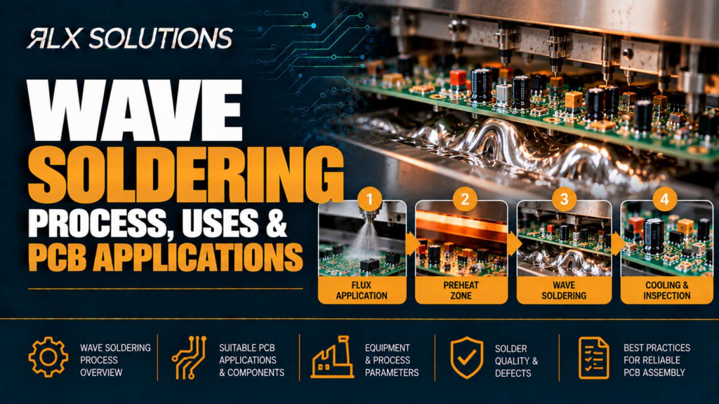
Wave Soldering: Process, Uses & PCB Applications
Wave soldering joins multiple through-hole component leads to a printed circuit board in one controlled pass over molten solder. RLX
Wave soldering joins multiple through-hole component leads to a printed circuit board in one controlled pass over molten solder. RLX
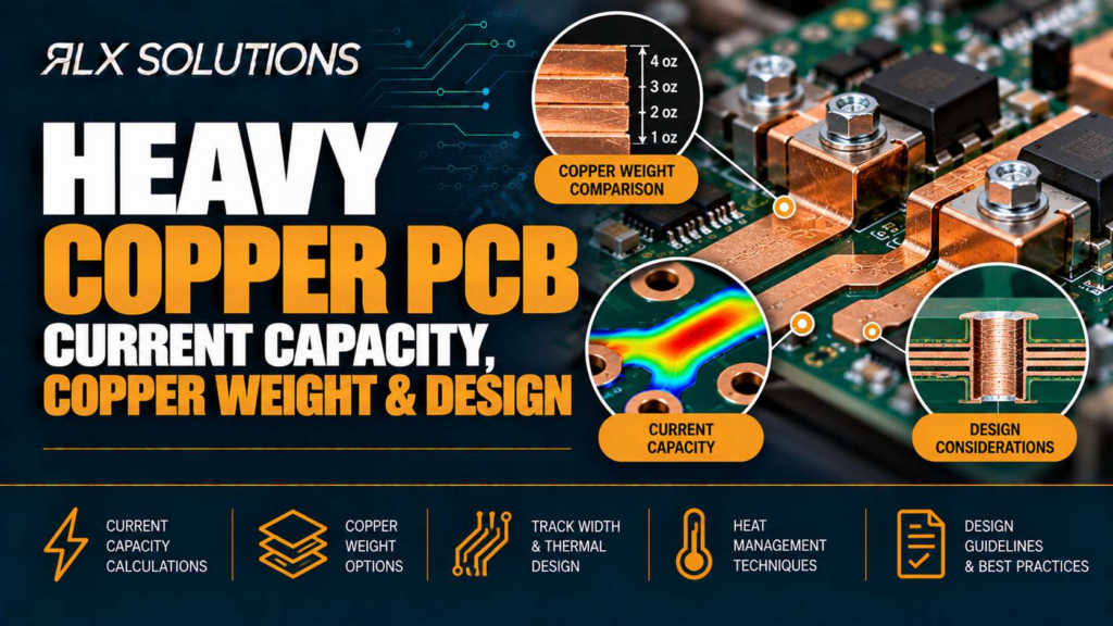
Heavy copper PCB current capacity depends on more than copper weight. Trace width, layer position, temperature rise, current path length,
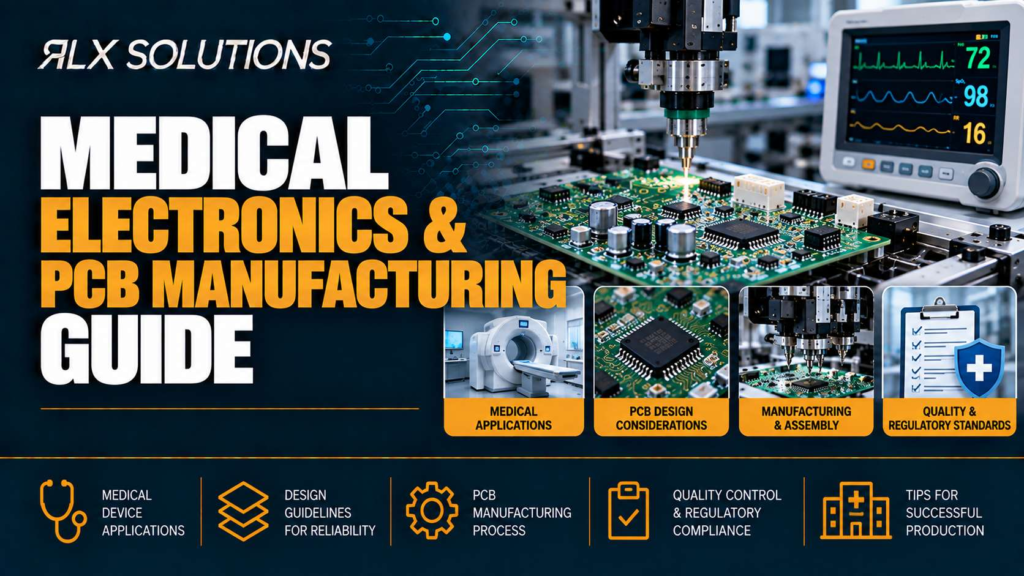
Medical electronics PCB manufacturing requires more than placing components on a circuit board. Design decisions affect fabrication, soldering, inspection, test
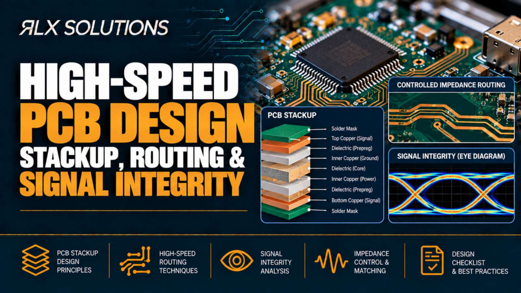
High-speed PCB design works when stackup, routing geometry and return paths are engineered as one system rather than three separate
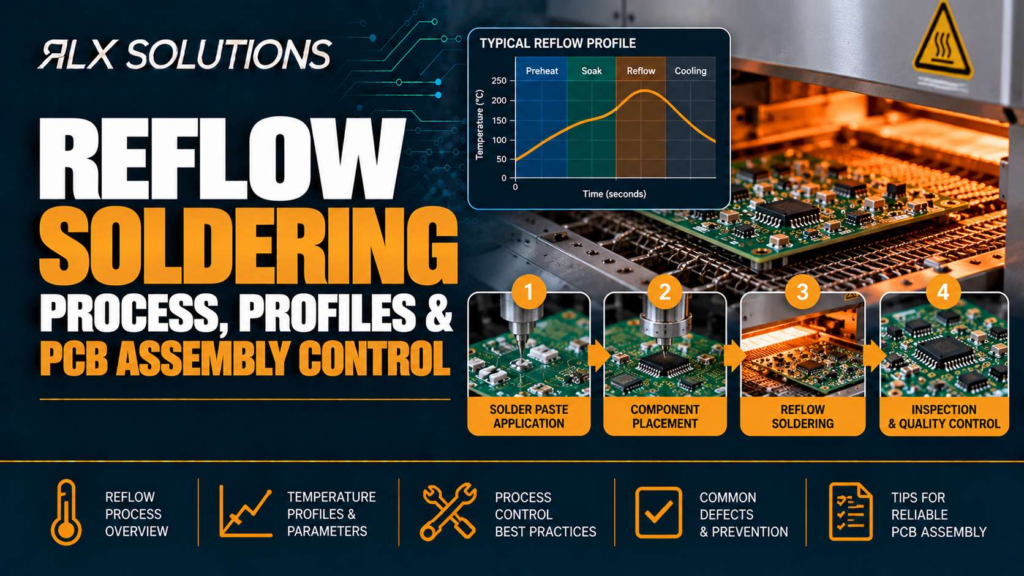
Reflow soldering joins surface-mount components to a printed circuit board by printing solder paste, placing parts, and heating the assembly
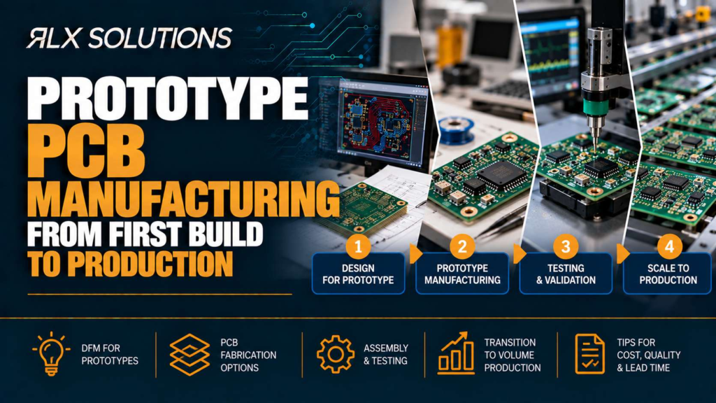
Prototype PCB manufacturing turns a design into hardware that can expose electrical, mechanical and manufacturing problems before they multiply at
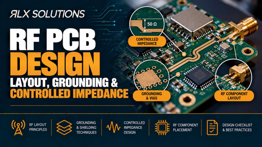
RF PCB design succeeds when the stackup, transmission-line geometry, return path and fabrication process are treated as one electrical system.
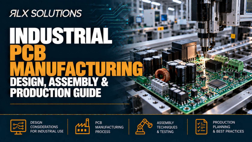
Industrial PCB manufacturing works best when design, bare-board fabrication, component sourcing, assembly and test are treated as one production system
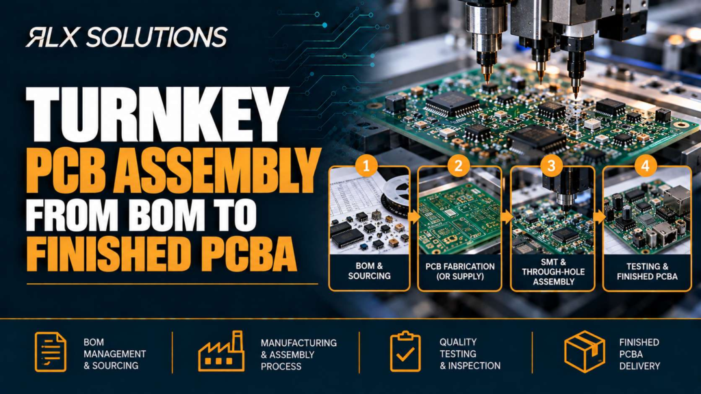
Turnkey PCB assembly puts component procurement, bare-board supply, assembly, inspection and test under one manufacturing programme instead of splitting them
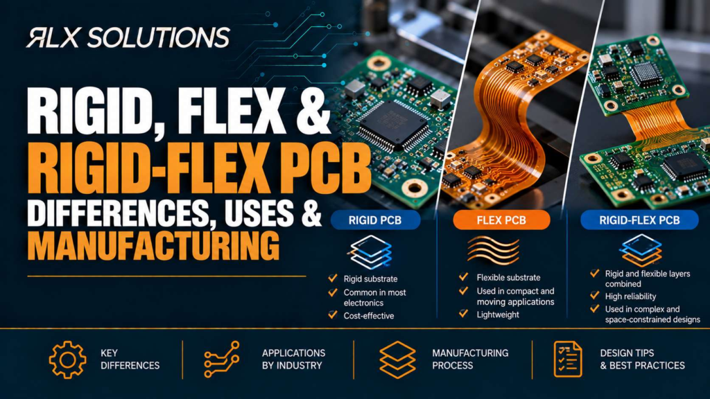
Rigid, flex and rigid-flex PCBs solve different mechanical and electrical packaging problems. Rigid boards provide a fixed structure, flex circuits