
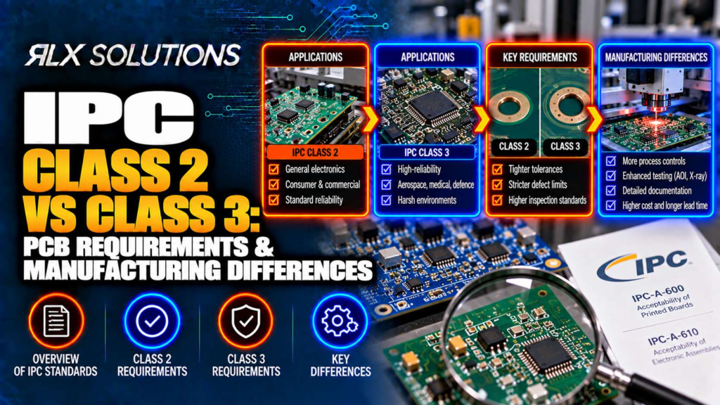
IPC Class 2 vs Class 3 is primarily a difference in the required level of manufacturing assurance, workmanship and acceptance criteria. Class 3 applies tighter fabrication and assembly requirements where continued performance matters more. RLX Solutions, a contract electronics manufacturer in Concord, Ontario, builds printed circuit boards to both classes.
The class decision reaches much further than final visual inspection. It affects how a bare PCB is fabricated, how solder joints are accepted, how inspection is performed and how the manufacturing record supports the finished assembly.
For an engineer, that means Class 3 should be treated as a design and procurement requirement from the beginning, not as a quality level added after the Gerbers and bill of materials (BOM) are released.
Class 2 and Class 3 target different performance expectations
IPC performance classes establish different acceptance expectations for electronic products. Class 2 is associated with products where continued performance and extended life are desired, while Class 3 applies where continued high performance or performance on demand is important.
The practical manufacturing distinction is assurance. A Class 3 circuit board has tighter criteria applied to features and workmanship that can influence long-term electrical or mechanical reliability.
That difference appears across both sides of PCB manufacturing.
For the bare board, IPC-6012 governs qualification and performance requirements for rigid printed boards. Moving from Class 2 to Class 3 tightens criteria such as annular ring and plating requirements.
After components are assembled, IPC-A-610 provides acceptability criteria for electronic assemblies. J-STD-001 addresses requirements for soldered electrical and electronic assemblies. These documents serve different purposes, so specifying “IPC Class 3” without identifying the applicable fabrication and assembly requirements can leave the purchase package open to interpretation.
| Manufacturing factor | Class 2 | Class 3 |
|---|---|---|
| Intended performance level | Continued performance and extended life | Continued high performance or performance on demand |
| Bare PCB fabrication | IPC-6012 Class 2 | IPC-6012 Class 3 |
| Annular ring criteria | Less restrictive | Tighter |
| Plating criteria | Standard Class 2 acceptance | Tighter Class 3 requirements |
| Assembly workmanship | IPC-A-610 Class 2 | IPC-A-610 Class 3 |
| Soldering requirements | Defined separately through applicable soldering requirements | Greater process attention where Class 3 requirements apply |
| Inspection burden | Appropriate to Class 2 acceptance | Greater verification against tighter criteria |
| Documentation impact | Defined by the purchase requirements | Often requires stronger evidence that specified requirements were met |
The important purchasing point is that Class 3 is not shorthand for “better PCB.” It is a defined performance class that changes which manufacturing conditions are acceptable.
Annular ring shows why Class 3 starts in PCB layout
An annular ring is the copper surrounding a drilled hole on a PCB layer. Its reliability depends on several manufacturing variables arriving in the right place at the same time: the drilled hole, the copper pad and the finished plating structure.
This makes annular ring a useful example of why Class 3 cannot simply be imposed at outgoing inspection.
Consider a hypothetical 8-layer, 1.6 mm board with a plated through-hole connecting Layer 1 through Layer 8. The designer selects a 0.30 mm finished hole and places it inside a copper land.
The drill does not exist in a mathematically perfect coordinate system. Registration, drilling and imaging all consume part of the geometric allowance around that hole. If the pad is reduced to gain routing space, less copper remains available to absorb those manufacturing variations.
Under Class 3, tighter annular ring requirements make that margin more significant. A layout that comfortably supports a Class 2 build can therefore require a pad, routing or via-architecture change before it is a sensible Class 3 design.
The downstream consequence can be expensive. Discovering insufficient geometry during fabrication review may force a layout revision. Discovering a related acceptance problem after boards have already moved through fabrication can put finished material at risk instead.
This is why the performance class belongs in the fabrication notes and design review before manufacturing begins.
Plating requirements change the fabrication control problem
A plated through-hole is formed by drilling the laminate and depositing conductive material on the hole wall before subsequent copper plating builds the required structure. The finished barrel becomes the electrical connection between layers.
Class 3 applies tighter plating criteria than Class 2. That matters because the finished connection is partly hidden inside the board.
Take a hypothetical 2.0 mm thick circuit board using a 0.20 mm mechanical drill. The nominal drill aspect ratio is 10:1, calculated from board thickness divided by drill diameter.
Now compare that with the same 2.0 mm board using a 0.40 mm drill. Its nominal aspect ratio is 5:1.
Both holes pass through the same stackup, but the 10:1 geometry presents a more demanding plating condition. Copper must form down a narrower, deeper barrel. A tighter performance class does not change the geometry, but it changes the importance of proving that the resulting structure satisfies the specified acceptance requirements.
That relationship between design geometry and process control is easy to miss when Class 3 is treated as an inspection note rather than a manufacturing input.
The same layer count can produce very different Class 3 builds
Layer count is a poor proxy for PCB manufacturing difficulty. Via architecture, lamination sequence, hole geometry, copper distribution and feature density can matter more.
Consider two hypothetical 10-layer boards of equal overall thickness.
| Decision factor | Board A | Board B |
|---|---|---|
| Layer count | 10 | 10 |
| Board thickness | 1.6 mm | 1.6 mm |
| Main via structure | Through vias, Layer 1 to Layer 10 | Laser microvias plus buried vias |
| Microvia structure | None | Layer 1 to Layer 2 and Layer 2 to Layer 3 |
| Buried structure | None | Layer 3 to Layer 8 |
| Example BGA pitch | 0.8 mm | 0.4 mm |
| Lamination demand | Conventional multilayer sequence | Sequential processing required by blind structures |
| Manufacturing consequence | Fewer interconnect process stages | More drilling, plating, filling and lamination dependencies |
Board B can cost more to manufacture even though the layer count is identical.
Its Layer 1 to Layer 2 and Layer 2 to Layer 3 microvias introduce laser drilling and HDI process steps. The Layer 3 to Layer 8 buried structure must be formed before the outer stack is completed. If microvias terminate in component pads, via-in-pad construction can also require resin filling, copper capping and planarization before component placement.
For Class 3, the lesson is not that complex via structures are prohibited. It is that every added manufacturing stage creates another feature whose geometry and workmanship must satisfy the required acceptance level. A quote based mainly on layer count can hide that difference.
Class 3 assembly changes what inspectors can accept
Fabrication class and assembly workmanship are related but distinct requirements. A bare board built to IPC-6012 Class 3 does not by itself establish that the populated assembly satisfies IPC-A-610 Class 3 workmanship requirements.
Assembly adds solder paste printing, component placement, reflow, through-hole processing and other operations. Each can create defects that did not exist on the bare board.
For surface-mount technology (SMT), solder paste inspection can identify paste volume, area and offset before reflow. Automated optical inspection can then evaluate visible post-reflow conditions. Packages such as ball grid arrays (BGAs), land grid arrays (LGAs) and quad-flat no-lead (QFN) devices create another problem: critical solder interfaces can be hidden underneath the package.
X-ray inspection provides visibility into those concealed connections.
Imagine a hypothetical 6-layer board with a 0.5 mm pitch BGA. Optical inspection can verify placement and surrounding visible features, but it cannot directly see every solder connection under the package. X-ray inspection becomes an important part of verifying conditions that optical methods cannot observe.
The class requirement therefore has to flow from the fabrication drawing into the assembly documentation and inspection plan. Otherwise, one supplier can build the bare board to one requirement while another interprets the populated assembly differently.
Class 3 increases the value of cross-section evidence
Some PCB characteristics cannot be established adequately from the outside of the finished board. Cross-sectioning turns an internal structure into a visible sample by cutting, mounting and polishing a representative section for examination.
That can expose features such as plated hole structure, internal registration and other construction details that external visual inspection cannot directly show.
For Class 3 fabrication, cross-section sampling supports verification of tighter requirements. It also illustrates an important cost mechanism: assurance consumes manufacturing resources.
A coupon or sample must be processed, prepared, inspected and documented. If a result identifies a nonconforming condition, the impact may extend beyond the inspected sample because the underlying process produced an entire lot.
That is different from simply spending more time looking at the finished PCB. Class 3 changes the evidence needed to demonstrate that hidden manufacturing features meet the specified requirements.
Do not confuse IPC-6012, IPC-A-610 and J-STD-001
A purchase order that says only “IPC Class 3” can be less informative than it appears. Engineers and buyers should identify which requirements apply to the bare board and which apply to the assembled product.
IPC-6012 addresses qualification and performance requirements for rigid printed boards. This is where the fabrication class becomes relevant to features such as annular rings and plating.
IPC-A-610 addresses the acceptability of electronic assemblies. It is commonly used to evaluate assembled workmanship.
J-STD-001 addresses requirements for soldered electrical and electronic assemblies. It is concerned with producing acceptable soldered interconnections, rather than serving as an interchangeable substitute for IPC-A-610.
These standards work at different points in the manufacturing chain. Treating them as synonyms can produce a documentation gap between PCB fabrication and assembly.
A complete release package should make the intended requirements clear enough that fabrication, assembly, inspection and purchasing teams are working to the same product definition.
Class 3 should be specified before the design is released
The cheapest point to resolve a Class 3 problem is usually before physical manufacturing starts.
For a new PCB, the manufacturer needs enough information to evaluate the design against the intended build. That commonly means providing:
- Gerber RS-274X, ODB++ or IPC-2581 fabrication data.
- NC drill data.
- The intended stackup.
- Impedance targets where controlled impedance is required.
- Fabrication notes identifying the applicable performance class.
- For assembly, the BOM, pick-and-place or centroid data, and assembly drawing.
- Any project-specific inspection, test and traceability requirements.
The engineer-reviewed design for manufacturability (DFM) review should then look beyond whether traces physically fit between pads. Via geometry, annular ring margin, drill aspect ratio, sequential lamination, via-in-pad construction and other process-sensitive features need to be considered against the proposed stackup.
A design that reaches purchasing without those decisions can generate quotes that appear comparable while assuming different manufacturing scopes.
Class 3 can increase cost without changing the schematic
Moving from Class 2 to Class 3 does not necessarily add a resistor, change a net or alter the electrical function of the schematic. It can still change manufacturing cost.
The mechanism is process assurance.
Tighter acceptance requirements can demand greater attention to fabrication control, sampling, inspection and documentation. If the PCB geometry leaves little process margin, the class change can also expose design changes that were unnecessary under the original requirement.
Consider a hypothetical 12-layer board that is electrically unchanged between two revisions. Revision A is released for Class 2. Revision B requires Class 3 but retains the same dense through-via field and routing.
The BOM is identical. The netlist is identical. The board outline is identical.
Yet Revision B must be evaluated against the tighter Class 3 requirements. If annular ring margin or another fabrication feature does not support that requirement, the commercial consequence starts with engineering work and can extend to layout changes and a new manufacturing review.
That is why comparing Class 2 and Class 3 pricing solely by PCB area, layer count and quantity misses part of the cost equation.
Put the class requirement into the supplier conversation early
For an OEM, the useful question is not “Can this supplier make Class 3 boards?” It is whether the proposed design, manufacturing process, inspection plan and documentation all support the requirement you are placing on the finished product.
That discussion becomes especially important with HDI structures, high aspect-ratio holes, fine-pitch packages, via-in-pad and controlled impedance. Each introduces manufacturing dependencies that need to be evaluated alongside the performance class.
If you are preparing a Class 2 or Class 3 circuit board for production, RLX reviews DFM as part of every quote. Send the complete fabrication package and, for assembly, the BOM and placement data so the class requirement can be reviewed against the actual build rather than treated as a note added at the end.
FAQ
Is IPC Class 3 always better than Class 2?
They represent different performance and acceptance requirements rather than a simple good-versus-better scale. Class 3 applies tighter criteria in areas such as annular ring and plating. The appropriate class should come from the product’s specified requirements, because selecting Class 3 also affects fabrication control, inspection and documentation.
Can a Class 2 PCB design be manufactured as Class 3 without changing the layout?
Sometimes the existing geometry may support the tighter requirement, but the class cannot safely be changed by editing the fabrication note alone. Annular rings, hole geometry, stackup and other manufacturing features should be reviewed against the Class 3 requirement before release. A layout created around Class 2 margins may need revision.
Does a Class 3 bare PCB automatically make the assembly Class 3?
No. Bare-board fabrication and electronic assembly are governed by different requirements. IPC-6012 applies to rigid printed board fabrication, while IPC-A-610 addresses electronic assembly acceptability and J-STD-001 addresses soldered electrical and electronic assemblies. The required class and applicable standards should therefore be identified through the manufacturing package.
Does Class 3 require a different PCB material?
Class 3 is a performance class, not a laminate family. Material selection remains a separate engineering decision driven by electrical, thermal, mechanical, regulatory and manufacturing requirements. The important manufacturing issue is whether the complete stackup and its resulting features can satisfy the specified Class 3 fabrication requirements.
Why can two Class 3 PCBs with the same layer count cost differently?
Layer count captures only part of manufacturing difficulty. A 10-layer board using through vias can require fewer process stages than a 10-layer HDI board using blind microvias, buried vias, sequential lamination and via-in-pad processing. The additional operations create manufacturing and inspection dependencies even before the performance class is considered.



Pingback: IPC-6012 Explained: PCB Fabrication Acceptance | RLX