
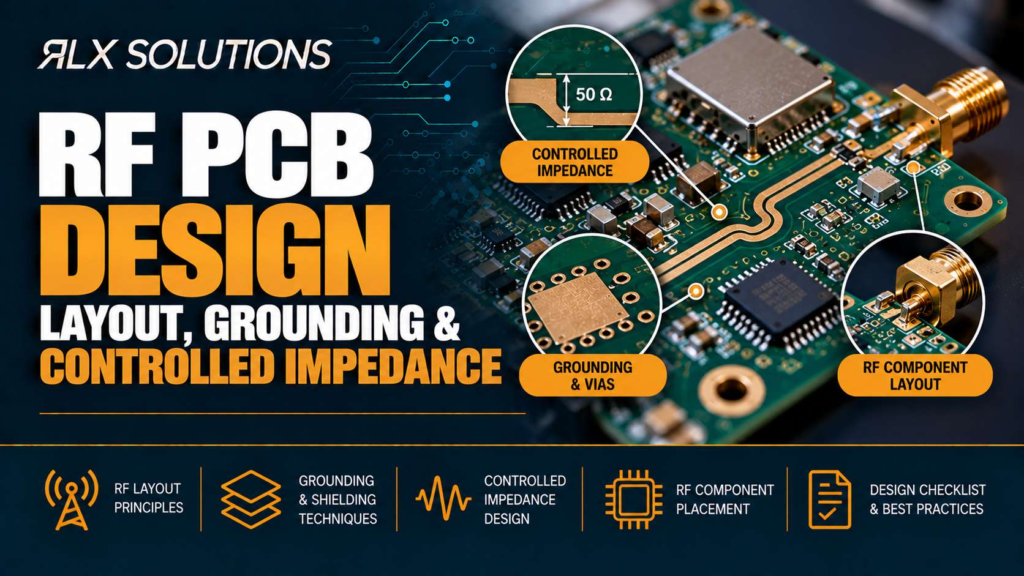
RF PCB Design: Layout, Grounding & Controlled Impedance
RF PCB design succeeds when the stackup, transmission-line geometry, return path and fabrication process are treated as one electrical system.
RF PCB design succeeds when the stackup, transmission-line geometry, return path and fabrication process are treated as one electrical system.

Industrial PCB manufacturing works best when design, bare-board fabrication, component sourcing, assembly and test are treated as one production system
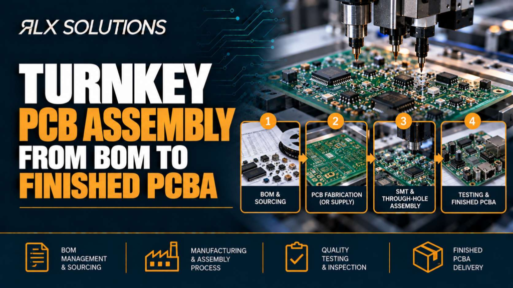
Turnkey PCB assembly puts component procurement, bare-board supply, assembly, inspection and test under one manufacturing programme instead of splitting them

Rigid, flex and rigid-flex PCBs solve different mechanical and electrical packaging problems. Rigid boards provide a fixed structure, flex circuits
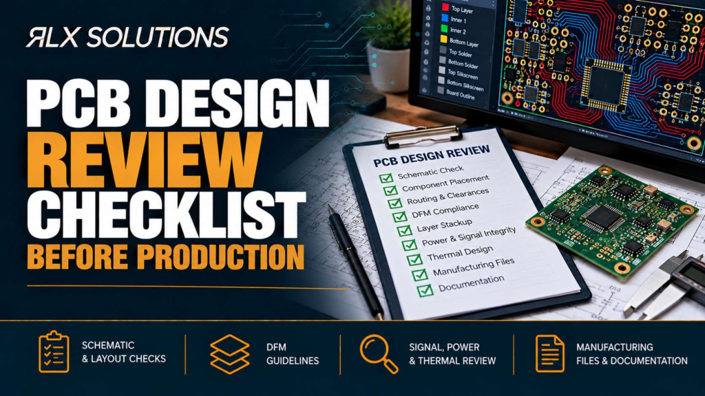
A PCB design review before production should confirm the stackup, drill plan, copper geometry, impedance targets, component data, assembly clearances,
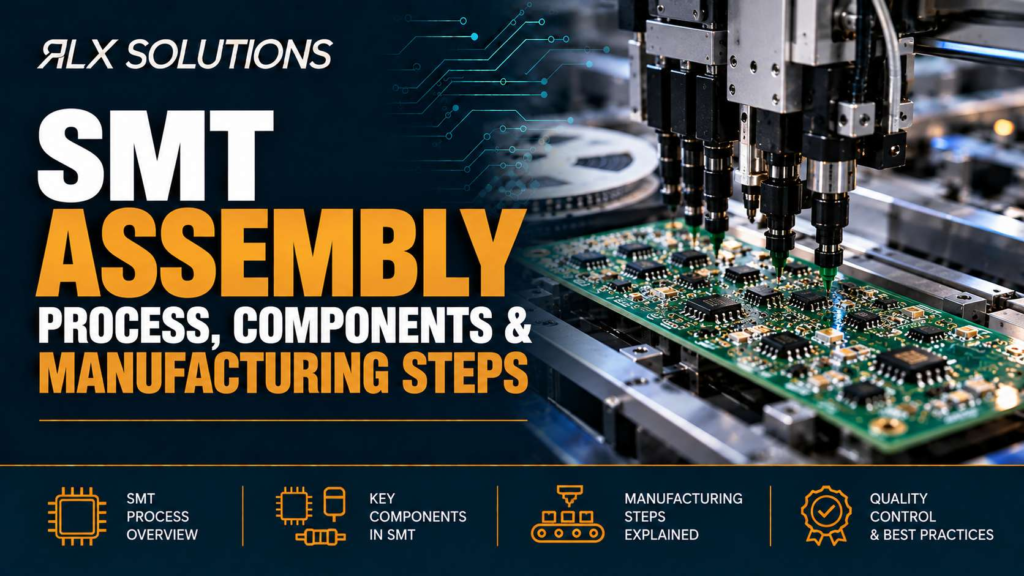
SMT assembly is the process of printing solder paste, placing surface-mount components, reflowing the solder, and inspecting and testing the

LED PCB manufacturing starts with heat, not routing density. The board must move heat away from the LED package while
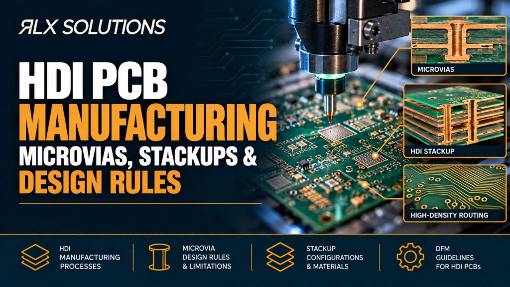
High-density interconnect (HDI) PCB manufacturing uses laser-drilled microvias, finer routing and engineered stackups to escape dense components without forcing every
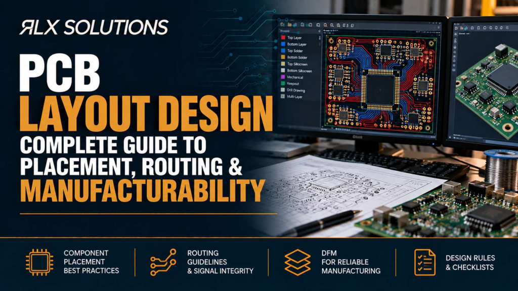
PCB layout design turns a schematic into a physical circuit board by assigning component locations, copper geometry, layer usage, vias,

Quick-turn PCB assembly succeeds when the build is ready to manufacture before the clock starts: complete fabrication data, a clean