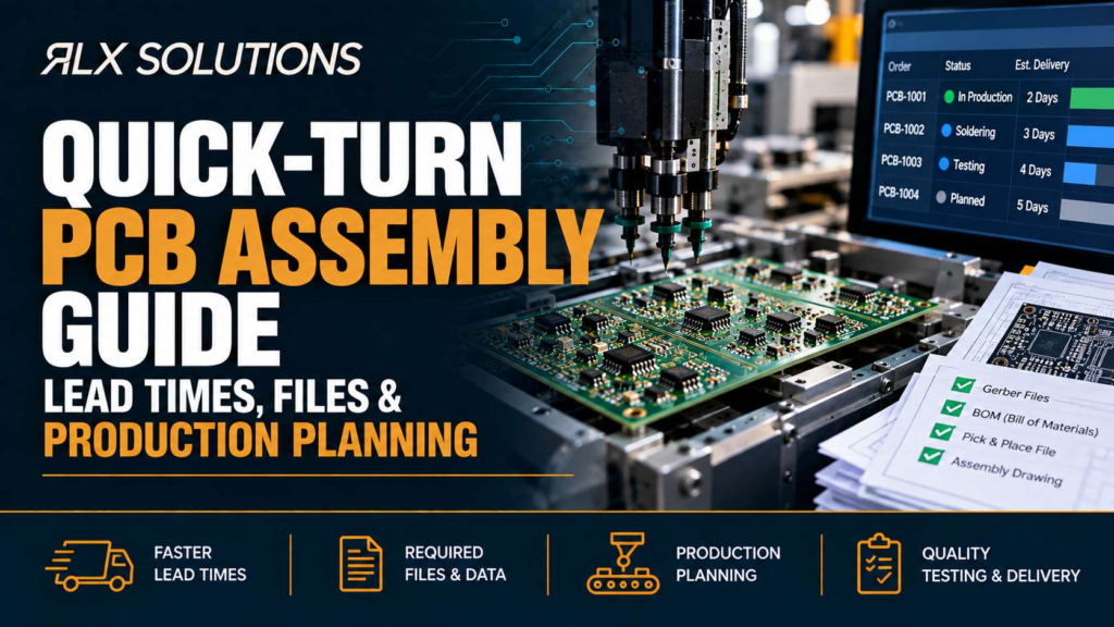
PCB cost is driven by the manufacturing steps required to fabricate the bare board, source components, assemble, inspect, test, and prepare the build. A smaller board can cost more than a larger one if it needs denser interconnects or extra process stages.
RLX Solutions, a contract electronics manufacturer based in Concord (Vaughan), Ontario, has an engineer review the full file package for its PCB assembly builds, where cost follows the process route, covering SMT, through-hole and mixed technology from prototype through production.
A useful cost model separates recurring work from work performed once for a build. Bare-board construction, components, placement, soldering, inspection, and test repeat with production. Engineering review, programming, tooling, machine setup, and some test preparation can behave more like fixed build-level work. That distinction explains why two boards with similar dimensions can produce very different commercial outcomes.
Start With the Bare Board Manufacturing Route
The cost of PCB board production begins with the physical route required to turn laminate and copper into the released design. Board area matters, but it is only one input. Layer count, copper weight, drill structure, trace geometry, material, surface finish, controlled impedance, and panel utilization can each change the amount of processing required.
A conventional multilayer board may move through imaging, etching, lamination, drilling, plating, solder mask, surface finish, profiling, and inspection. Add blind vias or stacked microvias and the sequence changes. Additional lamination and drilling operations can appear before the board reaches final finishing.
This is why engineers should think in process steps rather than isolated specifications. A requirement that adds one extra manufacturing stage can affect the commercial structure of every board in the lot.
Key bare-board drivers include:
- Layer count: More layers require additional inner-layer processing, registration control, and lamination work.
- Via architecture: Through vias are simpler than constructions that require blind vias, buried vias, microvias, or via-in-pad processing.
- Copper weight: Thicker copper changes etching behaviour and can force wider trace and spacing rules.
- Fine geometry: Narrow traces, tight spaces, small holes, and dense fanout reduce process margin.
- Material choice: Standard FR-4 and specialized high-frequency or thermal materials follow different material and processing paths.
- Surface finish: Finish selection affects final board processing and solderability requirements.
- Controlled impedance: Impedance-controlled designs require a defined stackup and verification method rather than artwork alone.
The main commercial point is simple: fabrication cost follows manufacturing work. Board dimensions describe the object, but the stackup and feature set describe how difficult it is to build.
PCB Cost Changes When the Same Layer Count Uses a Harder Stackup
Layer count is useful for early screening, but it does not explain total manufacturing cost. Two 10-layer boards can require very different process routes even when their outer dimensions are identical.
Consider this hypothetical comparison.
| Decision factor | Board A | Board B |
|---|---|---|
| Layer count | 10 layers | 10 layers |
| Outer copper | 1 oz | 1 oz |
| Routing | 4 mil / 4 mil | 3 mil / 3 mil |
| Via structure | Through vias only | Layer 1 to 2 and Layer 2 to 3 microvias plus buried vias |
| BGA escape | Conventional fanout | Via-in-pad |
| Filled and capped vias | No | Yes |
| Lamination route | Conventional multilayer sequence | Sequential lamination required |
Board B needs more manufacturing operations even though the layer count is unchanged. Laser drilling adds a different hole-forming step. Buried vias must be created before the complete multilayer structure exists. Via-in-pad may require resin fill, copper cap, and planarization before component pads are ready for assembly.
The extra work also creates more inspection points. If a buried connection is formed incorrectly, the defect can become inaccessible after later lamination. Process control therefore moves earlier in the build.
The purchasing lesson is that a request for quotation should describe the actual stackup and via spans. A line item that says “10-layer PCB” does not contain enough information to explain manufacturing effort.
Fine Features Affect Yield Risk and Process Margin
The question “how much does a PCB cost” is often answered too broadly because the design is treated as a collection of dimensions. Fine geometry changes the process window.
Take a hypothetical 6-layer, 1.6 mm board using 3 mil / 3 mil routing around a dense device. If a redesign can move the dense escape region to a less restrictive geometry without changing electrical performance, fabrication may become easier because imaging and etching have more margin. If the same redesign requires a 0.10 mm microvia structure to reach inner routing channels, part of that gain can be offset by laser drilling and related via processing.
Hole geometry produces a similar effect. A 0.20 mm finished hole through a relatively thick board has a different plating challenge from a larger hole through the same thickness. As aspect ratio rises, plating the hole wall consistently becomes harder because chemistry must reach deeper into the barrel.
This does not mean small holes or dense routing should be avoided. It means they should be used where the electrical or mechanical design requires them. Cost control works best when complexity is concentrated in the areas that need it rather than applied across the entire board.
Material, Copper, and Finish Decisions Can Change More Than Material Spend
Material selection changes fabrication behaviour as well as purchasing input. A high-frequency laminate, metal-core construction, or high-Tg material can affect drilling, lamination, handling, and stackup engineering. The material decision therefore belongs in the manufacturing discussion early.
Copper weight has a direct process consequence. As copper becomes thicker, etching narrow conductors and gaps becomes harder because copper is removed laterally as well as vertically. A design that combines heavy copper with fine routing may force a layout compromise or a more demanding process route.
Surface finish has a different role. It protects exposed copper and creates the solderable interface used later in assembly. Finish should be chosen for the component set, storage expectations, assembly process, and any contact requirements rather than treated as a cosmetic selection.
For procurement, the useful question is not which specification sounds more capable. Ask which requirement the product actually needs. Every unnecessary manufacturing constraint narrows the process window without creating product value.
Assembly Work Begins Before Placement
PCB assembly cost includes more than the time a placement machine spends installing components. The assembly process starts with data preparation, material control, solder paste printing, programming, line setup, inspection planning, and first-article verification.
The bill of materials (BOM), pick-and-place data, assembly drawing, and bare-board manufacturing files must describe the same revision. A complete-looking package can still create work if one file is stale or if component references do not agree.
Assembly effort is shaped by factors such as:
- component count and package mix
- single-sided versus double-sided population
- surface-mount technology (SMT), through-hole, or mixed assembly
- fine-pitch packages and hidden solder joints
- moisture-sensitive device handling
- programming requirements
- manual operations
- conformal coating, underfill, or potting
- inspection depth
- electrical and functional test requirements
Placement count matters because each component has to be handled and installed, but it does not tell the whole story. A board with fewer placements can require more manufacturing attention if it uses fine-pitch bottom-terminated packages, extensive through-hole work, or specialized post-assembly processes.
Package Choice Can Move Cost Into Inspection
Component packages can change what can be verified after soldering.
Consider a hypothetical controller board using a 0.3 mm-pitch ball grid array (BGA) plus conventional passives. Automated optical inspection can assess visible placement and solder features around the board, but the solder joints under the BGA are hidden from direct optical view. X-ray inspection addresses that physical limitation.
Now compare the same electrical function implemented with a package whose solder joints are visible from the side. Optical inspection has direct access to features that were hidden in the BGA case.
The cost mechanism is not that one package is “good” and another is “bad.” The package changes the inspection method required to gather evidence about the solder joints. Package selection can therefore affect manufacturing work after placement even if the component performs the same electrical function.
Component Sourcing Can Control the Commercial Result
The component list can contribute more to the total build than the bare circuit board. Availability, approved alternates, packaging, source traceability, and authenticity controls all matter.
A sourcing plan should define the exact manufacturer part number for critical devices and identify approved alternates where engineering permits them. If a component is obsolete, allocated, or available only through higher-risk channels, the procurement task can expand from purchasing into verification.
That verification can include source vetting, packaging inspection, lot checks, visual inspection, X-ray, electrical testing, or escalation to third-party analysis where required. These controls add work, but the alternative is allowing uncertain material into assembly.
Turnkey, kitted, and consigned builds also allocate sourcing responsibility differently. In a turnkey model, the manufacturer procures the material. In a kitted model, the customer may supply selected parts while the manufacturer sources the remainder. In a consigned model, the customer provides the complete kit.
The commercial comparison should therefore use the same sourcing scope. A quotation that excludes difficult components is not equivalent to one that includes them.
NRE Cost Comes From Work Performed Once for the Build
Non-recurring engineering (NRE) refers to work that is performed to prepare a design, process, fixture, program, or production method rather than repeated identically on every finished board.
In PCB work, NRE can arise from engineering review, tooling preparation, stencil creation, machine programming, inspection programming, fixture development, or test preparation. The exact mix depends on the build scope.
A hypothetical 20-board engineering run and a 200-board pilot may require similar preparation before the first acceptable assembly is released. If both require the same stencil, placement program, inspection setup, and functional test preparation, those build-level activities are spread across different quantities.
That is why unit economics can change with quantity even when the physical board is unchanged. The recurring work is still there, but fixed preparation is allocated across more finished assemblies.
The opposite risk also matters. If the design is still changing, committing to a larger quantity exposes more material and finished work to the next revision. A lower effective unit cost can be a poor decision if engineering risk is still high.
Inspection and Test Are Separate Cost Drivers
Inspection and test should be scoped by what each stage can detect.
Solder paste inspection (SPI) checks paste deposition before reflow. Automated optical inspection (AOI) checks visible assembly features after soldering. X-ray inspection is used where package construction hides joints that optical systems cannot see directly. Manual visual inspection adds human review against the required workmanship criteria.
Electrical test answers a different question. Flying-probe in-circuit test can verify nets without a dedicated bed-of-nails fixture, while fixture-based in-circuit testing can suit repeated production where the test strategy supports it. Functional test checks whether the assembled product meets customer-defined operating requirements.
These activities are not interchangeable. A functional test may show that a board powers up, but it may not identify every process defect. Optical inspection may verify visible solder quality, but it cannot prove firmware behaviour.
Procurement teams should compare quotations by test scope, not by a single line labelled “testing.” Two suppliers can quote the same assembly while proposing very different evidence for release.
Quantity Changes Cost Allocation, Not Process Physics
Higher quantity can spread fixed preparation across more assemblies, but it does not remove the operations required by the design.
A board that needs sequential lamination still needs sequential lamination. A BGA with hidden joints still needs an inspection method that can evaluate them. A programmed device still needs the required firmware process. Quantity changes how build-level work is allocated, not the physical steps required to make the product.
Low-volume PCB assembly has a separate planning problem because fixed setup work is distributed across a smaller batch. Our guide to small-batch assembly setup and release planning covers setup, first-article planning, and release quantity specifically, while this article focuses on the wider cost structure across bare-board fabrication and assembly.
For a new design, quantity should follow the maturity of the product. A smaller release can limit exposure while files, firmware, test methods, or mechanical interfaces are still being proven. Once those inputs are stable, a larger release can distribute preparation across more finished units.
Send Enough Data to Quote the Actual Build
A useful quotation is based on a complete manufacturing definition rather than assumptions.
For bare-board fabrication, send the released manufacturing data and the information needed to define the stackup, drilling, impedance, finish, and fabrication requirements. Common fabrication data formats include Gerber RS-274X, ODB++, IPC-2581, and NC drill files.
For assembly, add:
- BOM in .xlsx or .csv format
- pick-and-place or centroid data
- assembly drawing
- programming requirements where applicable
- test procedure and pass/fail criteria where applicable
- any customer-supplied material responsibilities
A separate article on what a complete assembly quote package contains covers file completeness, BOM data, and manufacturing requirements in depth. The breakdown of layer count and stackup effects on fabrication explains how layer construction changes multilayer manufacturing work, and the engineer-reviewed DFM process for catching production issues shows how design review identifies problems before release.
A complete package lets engineering separate true design requirements from assumptions. That makes the quotation easier to compare because the fabrication, sourcing, assembly, inspection, and test scope is visible.
Send Your Files for an Assembly Quote
Gerbers, BOM, pick-and-place. An RLX engineer reads every inquiry and replies with DFM/DFA feedback and any BOM flags before your build is quoted. RLX Solutions works under an ISO 9001:2015 certified quality system. Request a quote or send your files to sales@rlxsolutions.com.
Frequently Asked Questions
What is the biggest factor that affects PCB cost?
There is no single driver across every design. Bare-board construction, via architecture, copper, material, component sourcing, assembly process, inspection, test, and build-level setup can all change manufacturing work. For a simple board, components may dominate. For a dense multilayer design, fabrication steps such as sequential lamination or filled vias may have greater influence.
Why can two PCBs with the same dimensions cost differently?
Board dimensions do not describe the complete manufacturing route. Two boards with the same outline can use different layer counts, copper weights, materials, drill structures, trace geometry, finishes, and impedance requirements. Each difference can add processing or reduce manufacturing margin. The released stackup and feature set are therefore more useful than board area alone for quotation.
Does a higher layer count always make a PCB more expensive?
More layers normally add fabrication work, but layer count alone does not determine the commercial result. A 10-layer board with conventional through vias can follow a simpler route than another 10-layer design using microvias, buried vias, via-in-pad, and sequential lamination. Compare the complete construction rather than treating the layer count as a standalone predictor.
Why does PCB assembly become more expensive with fine-pitch components?
Fine-pitch and bottom-terminated packages can add process control and inspection requirements. Placement accuracy, solder paste deposition, reflow behaviour, and hidden-joint inspection may all require additional attention. A BGA, for example, hides its solder joints beneath the package, so direct optical inspection cannot evaluate those connections in the same way it can inspect visible leads.
What files should I send to get a PCB quotation?
For fabrication, send released manufacturing data such as Gerber RS-274X, ODB++, IPC-2581, or NC drill files plus the stackup and applicable fabrication requirements. For assembly, add the BOM, pick-and-place or centroid data, and assembly drawing. Include programming and test requirements when they form part of the build so the quotation reflects the intended manufacturing scope.