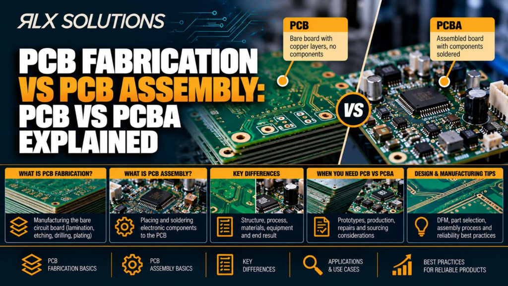
PCB fabrication produces the bare printed circuit board, while PCB assembly mounts and solders electronic components onto that board to create a functional assembly, often called a PCBA. For engineers sourcing both stages, RLX Solutions, a contract electronics manufacturer in Concord, Ontario, treats them as connected manufacturing processes with different inputs, controls and failure modes.
PCB Fabrication vs PCB Assembly at a Glance
The practical difference is where each process sits in the product build. Fabrication turns the PCB design into a physical circuit board. Assembly takes that fabricated board, adds the specified components and creates the electrical hardware that can be inspected, programmed and tested.
| Decision factor | PCB fabrication | PCB assembly |
|---|---|---|
| Starting point | PCB manufacturing data | Fabricated bare boards plus component data |
| Main output | Bare PCB | Populated circuit board, or PCBA |
| Primary inputs | Gerber, ODB++, IPC-2581, NC drill, stackup and fab notes | BOM, pick-and-place data, assembly drawing and bare boards |
| Main operations | Imaging, lamination, drilling, plating, etching, solder mask and surface finish | Solder paste, component placement, reflow, through-hole insertion and soldering |
| Geometry focus | Traces, spacing, holes, vias, copper and stackup | Package size, pad access, polarity, placement and solder joints |
| Common inspection targets | Board dimensions, holes, copper features and electrical nets | Paste deposits, placement, solder joints and hidden connections |
| Typical electrical test | Bare-board continuity and isolation | ICT, functional test and programming as required |
| Primary sourcing question | Can this PCB be manufactured to the specified geometry? | Can the correct components be sourced, placed, soldered and verified? |
The two stages are related but not interchangeable. A bare board can pass fabrication inspection and still create assembly problems if its footprint geometry, finish, component access or thermal design does not support the intended assembly process.
PCB Fabrication Builds the Electrical Structure
PCB fabrication converts digital manufacturing data into the physical copper and dielectric structure of a circuit board. On a multilayer PCB, that means more than printing traces. The manufacturer has to create and register internal layers, laminate the stack, drill holes and vias, plate conductive features, form the outer layers, apply solder mask and add the specified surface finish.
A plated through-hole connects conductive layers by depositing copper on the wall of a drilled hole. Blind vias terminate before crossing the complete board thickness, while buried vias connect inner layers without reaching either external surface. Those choices change the manufacturing sequence.
Consider an 8-layer, 1.6 mm board with conventional through vias. If every plated via passes from Layer 1 to Layer 8, drilling can occur after the multilayer structure is laminated. Change the design to include Layer 1 to Layer 2 microvias and a buried connection from Layer 3 to Layer 6, and the fabrication sequence changes. The internal structure and via connections must be built in the correct order rather than created with one final drilling operation.
That difference can affect both manufacturing risk and cost even though the finished designs still have eight copper layers.
Board A vs Board B: Same Layer Count, Different Manufacturing Work
| Factor | Board A | Board B |
|---|---|---|
| Layer count | 10 layers | 10 layers |
| Finished thickness | 1.6 mm | 1.6 mm |
| Via architecture | Through vias only | Layer 1 to 2 microvias, Layer 2 to 3 microvias and buried vias |
| Drilling approach | Mechanical through drilling | Laser microvia drilling plus internal via processing |
| Lamination sequence | Simpler multilayer build | Sequential processing required |
| Cost pressure | Fewer specialised operations | More drilling, plating and lamination stages |
| Main risk | Through-hole geometry and registration | Registration across multiple via and lamination stages |
Layer count alone is therefore a weak basis for comparing PCB prices. Two 10-layer boards can require very different process flows.
Aspect ratio matters for the same reason. A 0.20 mm hole through a 2.0 mm board has a 10:1 thickness-to-hole relationship. Reducing that hole to 0.15 mm without changing board thickness pushes the ratio above 13:1. That is not a cosmetic CAD change. The deeper, narrower hole makes drilling and reliable copper deposition more demanding, so hole geometry has to be reviewed with the stackup rather than treated as an isolated drill-table value.
PCB Assembly Turns the Bare Board Into Electronic Hardware
PCB assembly begins after the bare board exists. Components identified by the bill of materials (BOM) are placed onto their corresponding PCB footprints and electrically connected through solder joints or other specified termination methods.
For surface-mount technology (SMT), solder paste is deposited onto pads before placement. Components are then positioned and the board passes through reflow, where the solder paste forms the electrical and mechanical joints. Through-hole components require leads to pass through holes and use an appropriate soldering process. Mixed-technology assemblies combine both.
Assembly density changes the inspection strategy. A visible gull-wing lead can be inspected optically, while the solder connections beneath a ball grid array (BGA) are hidden after placement.
Take a six-layer PCB carrying a 0.5 mm-pitch BGA, several QFNs and 0402 passives. The bare board manufacturer is concerned with pad geometry, registration, vias, copper structure, mask definition and finish. Once assembly starts, solder paste deposition, component placement and hidden solder joints become additional process variables.
Solder paste inspection (SPI) before reflow can measure paste volume, area and offset. Automated optical inspection (AOI) after reflow checks visible placement and solder features. X-ray inspection is useful for packages such as BGA, land grid array (LGA) and QFN devices where important solder regions cannot be evaluated from the top of the board.
That inspection chain explains why a fabricated PCB passing its own acceptance checks does not establish that the assembled board will pass assembly inspection.
PCB vs PCBA: The Extra “A” Changes the Sourcing Scope
A PCB is the physical printed circuit board before electronic parts are assembled onto it. A PCBA is a printed circuit board assembly, meaning the PCB has been populated with components.
That distinction matters on a request for quotation. A PCB quote can be based primarily on board manufacturing data. An assembly quote has to account for the BOM, component availability, placement data, assembly instructions and test requirements in addition to the board itself.
For a PCBA request, the manufacturing package typically needs:
- PCB manufacturing data. Gerber RS-274X, ODB++, IPC-2581 or other accepted fabrication data defines the bare board.
- NC drill data. This identifies drilled features required by the PCB.
- Stackup and impedance information. These establish layer construction and controlled-impedance requirements where applicable.
- BOM. The component list identifies manufacturer part numbers and required quantities.
- Pick-and-place or centroid data. This defines component locations and rotations.
- Assembly drawing. This communicates assembly-specific requirements that machine placement data alone may not capture.
Missing or conflicting files create a handoff problem. A footprint may exist in the PCB data while the BOM calls for a different package, or a component rotation may conflict with the assembly drawing. Those discrepancies should be resolved before placement rather than discovered after components have been soldered.
Fabrication Cost and Assembly Cost Come From Different Decisions
Fabrication cost is driven by the structure that must be manufactured. Assembly cost is driven by what must be sourced, placed, soldered, inspected and tested.
For fabrication, decisions such as layer count, via architecture, board thickness, hole size, copper weight, fine trace geometry, material system and surface finish can alter the process route. A design using blind or buried vias, for example, may require processing that a through-via design avoids.
Assembly has another set of cost drivers. Component count, package density, fine-pitch parts, hidden solder joints, through-hole content, sourcing conditions, programming and test requirements all affect the work after fabrication.
Imagine two 4-layer boards measuring 100 × 80 mm. Both use 1 oz outer copper and conventional through vias. Board A has 35 components, mostly larger passives and leaded packages. Board B has 180 components, including a 0.5 mm-pitch BGA and multiple QFNs. Their bare-board fabrication requirements may be similar, but Board B creates substantially more placement, soldering and inspection work.
This is why comparing only bare PCB pricing can distort the economics of the finished product. A layout decision that saves space may add assembly or inspection requirements later.
Design for Fabrication and Design for Assembly Solve Different Problems
Design for manufacturability (DFM) asks whether the PCB geometry can be manufactured consistently. Design for assembly (DFA) asks whether components can be placed, soldered, inspected and handled effectively.
Fabrication review focuses on issues such as trace and spacing geometry, drill-to-copper relationships, annular rings, via structures, copper-to-edge clearance, stackup and impedance. Assembly review shifts attention toward footprints, component orientation, solder access, package density, thermal behaviour and inspection access.
The two reviews intersect at the land pattern. A via placed inside a BGA pad, for example, is both a PCB fabrication feature and an assembly decision. An open via can allow solder to migrate away from the joint during reflow. Resin filling, copper capping and planarization can create a flat via-in-pad surface suitable for component placement.
That is an example of a decision that cannot be assigned neatly to only fabrication or assembly. The board structure determines whether the assembly process has a usable soldering surface.
Inspection and Testing Continue After Fabrication
A bare PCB test establishes whether the manufactured interconnect corresponds to the intended electrical network. Assembly testing asks a different question: did the population and soldering process produce the intended assembled hardware?
Inspection may progress from SPI before reflow to AOI after reflow and X-ray for hidden joints. In-circuit test (ICT) can then verify electrical characteristics and net behaviour at the assembly level. Flying-probe ICT avoids a dedicated fixture for prototype and lower-volume work, while bed-of-nails ICT uses a fixture suited to production conditions.
Functional test (FCT) goes further by exercising the assembly against a customer-defined procedure. Programming can also become part of the production route when devices require firmware, bootloader loading or in-system programming.
This sequence matters during design. Test points omitted from the PCB cannot simply be added by the assembly line. If production test requires electrical access, that requirement belongs in the PCB design before fabrication begins.
Component Procurement Is Part of the PCBA Risk Model
PCB fabrication can proceed from manufacturing data without purchasing the electronic parts that eventually populate the board. Turnkey PCB assembly adds a supply-chain problem to the manufacturing problem.
The BOM has to translate into actual components with correct manufacturer part numbers, quantities and traceability. Obsolete, end-of-life, allocated or otherwise difficult parts can affect an assembly even when the bare PCB is straightforward to manufacture.
Counterfeit risk also changes the control plan. Source vetting, packaging and date-code checks, visual inspection, lot verification, X-ray and electrical testing can all become relevant depending on the sourcing route and risk associated with the part.
This creates an important design consequence: a footprint decision can become a sourcing constraint. If a design accepts only one difficult-to-source component with no approved alternative, the PCB may be easy to fabricate while the PCBA remains difficult to build.
Specify Fabrication and Assembly as One Manufacturing Chain
The cleanest handoff happens when fabrication, component data, assembly requirements and test intent agree before production starts.
For an engineer preparing a build, that means checking the PCB manufacturing package against the BOM and assembly data rather than treating them as independent document sets. Stackup changes can affect via geometry. Footprint changes can affect soldering. Component substitutions can affect package dimensions. Test strategy can require PCB access points.
If you are preparing a board for fabrication and assembly, RLX can review the manufacturing and assembly package as part of the quotation process. Send the applicable Gerbers or other accepted PCB data, BOM, pick-and-place file and assembly drawing so that fabrication, sourcing and assembly requirements can be reviewed together.
Frequently Asked Questions
Can a PCB work without PCB assembly?
A bare PCB provides the conductive paths, pads, holes and physical structure defined by the design, but it does not contain the electronic components needed to perform the intended circuit functions. PCB assembly adds those components and their electrical connections. Some bare-board electrical testing can occur before assembly, but that is different from operating the finished circuit.
What files do I need for a PCB assembly quote?
For the assembled product, provide the PCB manufacturing data along with the BOM, pick-and-place or centroid file and assembly drawing. Stackup, impedance targets and fabrication notes should also be included when applicable. Complete and internally consistent files allow the manufacturer to review the bare-board requirements, component population and assembly instructions together.
Does PCB assembly include component sourcing?
It can. A turnkey build places component procurement with the manufacturer, while a kitted build can combine customer-supplied critical parts with manufacturer-sourced components. In a consigned build, the customer supplies the complete kit. The appropriate model depends on who will control purchasing, inventory and component availability for the programme.
Is PCB testing the same as PCBA testing?
No. Bare-board testing verifies the PCB’s electrical interconnect before components are installed. PCBA inspection and testing address the populated assembly and can include SPI, AOI, X-ray, ICT and functional testing depending on the build. Each stage targets different failure mechanisms, so passing bare-board testing does not replace assembly-level verification.
When should I review assembly requirements during PCB design?
Before fabrication data is released. Assembly requirements can affect footprints, component orientation, via-in-pad treatment, solder access, inspection strategy and test-point placement. Reviewing those issues after the boards have been fabricated can turn a layout issue into rework, a board revision or a test-access problem that cannot be corrected on the assembly line.