PCB assembly turns a fabricated circuit board into a tested electronic assembly through controlled solder paste printing, component placement, reflow, through-hole insertion, soldering, inspection and test. RLX Solutions, a contract electronics manufacturer in Concord, Ontario, reviews these stages as one production flow because a decision made at placement can determine inspection, rework and test requirements later.
PCB assembly starts before the first component is placed
A PCB assembly build begins with the manufacturing data, not the placement machine. The assembler needs the bill of materials (BOM), pick-and-place or centroid data, assembly drawing and bare-board manufacturing files. For mixed-technology products, the drawing should also make the intended assembly sequence clear.
A bare PCB is the fabricated printed circuit board before components are installed. PCB assembly, often shortened to PCBA after the term has been introduced, is the process of installing, soldering, inspecting and testing those components.
Three sourcing models change who controls component procurement:
| Assembly model | Customer supplies | Manufacturer handles |
|---|---|---|
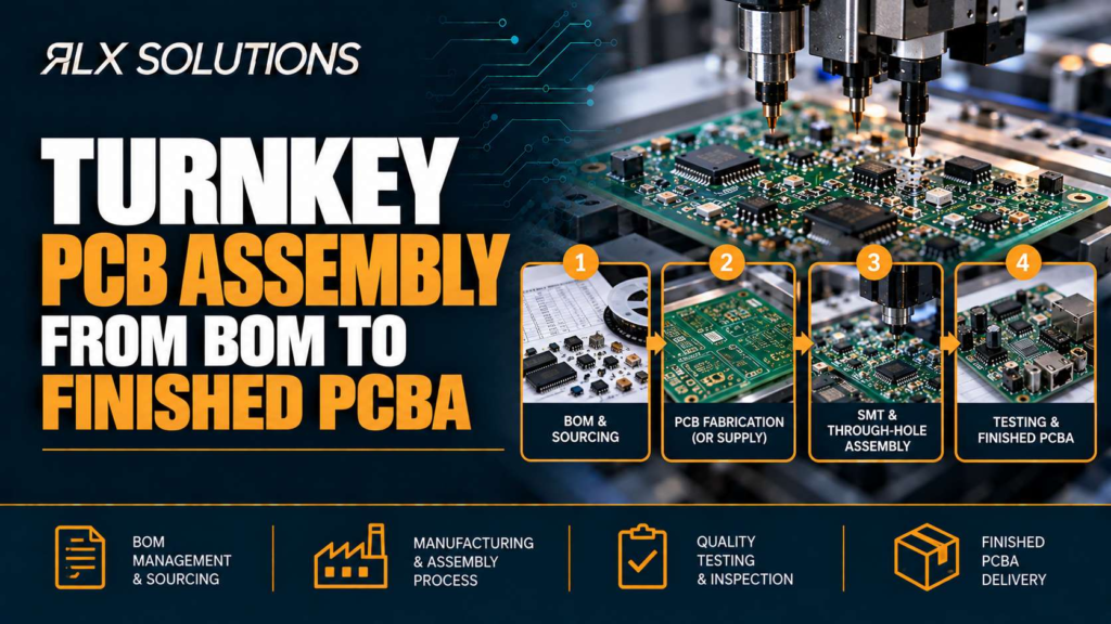
| Turnkey | Manufacturing data and product requirements | Component procurement, bare boards, assembly, inspection and test |
| Kitted or partial turnkey | Selected critical or long-lead parts | Remaining sourcing plus assembly and test |
| Consigned | Complete component kit | Assembly, inspection and test |
This distinction matters because a correct BOM does not guarantee a buildable kit. Date codes, moisture exposure, packaging condition, substitutions and part authenticity can affect the line before solder paste reaches the circuit board.
Incoming parts with counterfeit risk may therefore require source vetting, package inspection, date-code and country-of-origin checks, lot verification, X-ray, electrical testing or third-party analysis. Moisture-sensitive devices also need controlled handling and storage under the applicable moisture-management process. A component that absorbs moisture can fail during reflow even when its electrical specifications and manufacturer part number are correct.
Electrostatic discharge (ESD) controls serve a different purpose. ESD work zones protect sensitive components from electrical damage during handling, while moisture-sensitive device controls address absorbed moisture and reflow exposure. They solve separate failure mechanisms and should not be treated as interchangeable controls.
SMT assembly is a chain of linked process controls
Surface-mount technology (SMT) places components directly onto pads on the circuit board. The important point is that placement accuracy is only one part of the process. Paste deposition, component condition, pad geometry, thermal profile and inspection all influence the final solder joint.
1. Solder paste printing controls how much solder reaches the joint
A stencil deposits solder paste onto the surface-mount pads. Paste volume matters because the solder joint is formed from the material printed before placement.
Too little paste can produce an open or weak joint. Too much can increase bridging or create excess solder. Offset printing can leave a pad only partly covered even if the nominal stencil opening is correct.
Solder paste inspection (SPI) measures paste volume, area and offset before reflow. Checking the print at this stage isolates a process variable before components hide the pad.
That changes the economics of correction. Cleaning and reprinting a circuit board before placement is different from diagnosing a solder defect after reflow, component removal and rework.
2. Placement must match both pad geometry and package geometry
Pick-and-place equipment uses centroid data to position surface-mount components. The assembly drawing provides information that coordinate data alone may not communicate clearly, such as polarity, orientation and special handling notes.
Package density raises the consequences of small placement or print errors. Assembly may involve devices down to 01005 passives and ball grid arrays (BGAs) with pitches down to 0.3 mm. At those dimensions, an error may be difficult or impossible to judge from normal visual inspection alone.
Design for assembly (DFA) therefore begins in layout. Pad geometry, component spacing, polarity markings, fiducials and access for inspection all affect whether the intended build can be controlled repeatedly.
3. Reflow converts the paste deposit into a solder joint
After placement, the board passes through a reflow process. The thermal cycle heats the assembly so the solder paste activates, melts and wets the intended surfaces before cooling into the finished joint.
The mechanism is thermal, which means the board does not heat uniformly. A small passive beside a large copper region and a high-mass connector can experience different thermal behaviour even though both ride through the same oven.
This is why component density and copper distribution affect assembly rather than just bare-board fabrication.
A solder joint is the metallurgical and mechanical connection formed between a component termination and the PCB pad. Its quality depends on more than whether solder is visibly present. Wetting, alignment, joint shape and hidden interfaces also matter.
Hidden solder joints change the inspection strategy
Post-reflow automated optical inspection (AOI) can inspect visible component and solder features on both sides of the board. It is useful for detecting placement and visible solder defects, but optical systems cannot see through a package.
That limitation becomes significant with BGAs, land grid arrays (LGAs) and quad flat no-lead (QFN) packages. Their critical solder interfaces may sit beneath the component body.
Automated X-ray inspection (AXI) provides another view of those joints. It can be used for BGA and LGA connections, QFN thermal pads and void analysis.
The inspection method should follow the failure mode.
If a gull-wing lead is visibly misaligned, optical inspection can address the relevant feature. If a BGA ball is hidden beneath the package, adding more optical magnification does not change the fact that the joint is obscured.
Manual visual inspection under magnification remains part of the process for workmanship assessment to IPC-A-610 Class 2 or Class 3 requirements. Class 3 imposes tighter workmanship expectations than Class 2, so the intended build class needs to be established before production rather than treated as a final inspection preference.
Through-hole assembly solves a different mechanical problem
Through-hole technology inserts component leads or terminals through drilled holes in the circuit board. The joint is then soldered so the lead and plated hole form an electrical and mechanical connection.
Surface-mount and through-hole are therefore not simply old and new versions of the same assembly method. They create connections differently and often serve different package or mechanical requirements.
Through-hole assembly can appear on products with connectors, relays, large electromechanical parts or other components whose leads pass through the PCB. A mixed-technology board contains both surface-mount and through-hole components.
The process sequence matters. If through-hole parts block access to nearby surface-mount devices, installing them too early can complicate inspection or rework. If their thermal mass is high, their soldering process may also need to be considered separately from SMT reflow.
Selective soldering provides a way to solder targeted through-hole areas without subjecting the entire underside of an assembled board to the same solder contact. The value is process isolation: the soldering operation can be directed at the intended through-hole joints while already assembled regions are protected by the production plan.
Worked example: same PCB, different assembly sequence
Consider a hypothetical 6-layer, 1.6 mm circuit board with a 0.5 mm-pitch surface-mount controller on the top side and two through-hole connectors along one edge.
One sequence installs the connectors before all surface-mount inspection is complete. Their housings partially obstruct access to nearby components. A placement defect discovered later may now require working around the connector body.
A second sequence prints paste, places the SMT components, completes reflow and post-reflow inspection, then installs the two through-hole connectors and solders them selectively.
The layer count and board thickness did not change. What changed was access. The second process isolates the SMT verification step before the mechanical geometry of the connectors constrains inspection and rework.
Soldering method follows the component and assembly architecture
There is no single soldering operation that covers every populated PCB.
SMT components normally pass through solder paste printing and reflow. Through-hole parts require solder to form a connection through the plated hole. Mixed-technology designs may therefore combine reflow with selective soldering and manual soldering operations where appropriate.
J-STD-001 addresses soldering workmanship, while IPC-A-610 addresses acceptance of completed electronic assemblies. They are related, but they are not the same document. One governs process workmanship requirements around soldered electrical assemblies; the other is used to assess the acceptability of the resulting assembly.
This distinction matters during quoting and production planning. Specifying an assembly class without communicating the expected soldering and documentation requirements leaves part of the manufacturing intent unstated.
Two six-layer boards can carry very different assembly cost
Layer count is a poor shortcut for estimating assembly difficulty because assembly cost follows process steps, package density, inspection requirements and test strategy.
Consider these two hypothetical 6-layer boards:
| Decision factor | Board A | Board B |
|---|---|---|
| PCB structure | 6 layers | 6 layers |
| Smallest passive | 0603 | 01005 |
| Fine-pitch device | 0.8 mm-pitch BGA | 0.3 mm-pitch BGA |
| Through-hole parts | None | 3 connectors |
| Primary soldering | SMT reflow | SMT reflow plus selective soldering |
| Hidden joints | BGA joints | Fine-pitch BGA joints plus QFN thermal pad |
| Inspection demand | SPI, AOI, X-ray where required | SPI, AOI and greater reliance on X-ray |
| Assembly flow | SMT-dominant | Mixed technology |
Board B does not cost more because six layers somehow became harder to assemble. The added work comes from the assembly architecture.
The 01005 components put more sensitivity on paste deposition and placement. The 0.3 mm-pitch BGA increases the density of hidden solder connections. The QFN thermal pad introduces another solder interface that cannot be completely assessed by ordinary visual inspection. The three through-hole connectors add insertion and another soldering stage.
This is why assembly pricing cannot be read directly from a Gerber layer count. Two bare boards with similar fabrication complexity can create very different production routes after components are introduced.
First article approval separates setup from production release
A first article inspection (FAI) is the controlled evaluation of the first completed build before the remaining production lot is released.
That checkpoint matters because manufacturing data can be internally consistent and still encode the wrong intent. A centroid file can place a polarized component exactly where its coordinates specify while the rotation convention is wrong. A BOM can contain a valid manufacturer part number that does not match the footprint chosen in layout.
FAI gives the customer a defined opportunity to approve the physical implementation before the production lot continues.
For a new build, customer-signed first article approval should therefore be treated as part of the production gate, not merely as a sample shipped alongside production units.
Test coverage must be designed around what inspection cannot prove
Inspection and electrical test answer different questions.
SPI can verify solder paste deposition. AOI can identify visible placement and solder anomalies. X-ray can expose hidden package features. None of those methods proves that every electrical net performs correctly in operation.
In-circuit test (ICT) and functional test address that gap from different directions.
Flying-probe ICT can provide full net coverage for prototype and low-volume work without a dedicated fixture. Bed-of-nails ICT is suited to production when a test fixture is part of the manufacturing strategy.
Functional test (FCT) checks the assembly against the customer’s specified behaviour and can log pass or fail results with serial traceability.
Worked example: inspection success does not equal functional success
Take a hypothetical controller board using a 0.5 mm-pitch microcontroller, an 8-pin power device and a 20-pin connector.
SPI confirms acceptable paste deposition and AOI finds the visible components present and correctly oriented. Those results still do not prove that a programmed processor boots, that connector signals reach the intended nets or that the power section behaves according to the product specification.
Adding electrical test changes the question from “Does the assembly look correctly built?” to “Do its electrical connections or functions behave as required?”
The engineer needs to define the expected test behaviour. Functional testing is performed to the customer’s test specification, so limits, fixtures, firmware states, interfaces and pass/fail conditions should be resolved before production instead of being improvised after the first lot is assembled.
Programming and serialization belong in the production flow
Many assemblies are not complete when soldering ends.
In-system programming may use interfaces such as ISP/ICSP, JTAG or SWD for firmware and bootloader loading. Programming needs physical or electrical access to the relevant interface, so those connections should be considered during design rather than added after layout is locked.
Serialization creates another link between manufacturing and test. Serial markings, labels, laser marking or programmed identifiers such as MAC addresses can connect a physical unit to its production and test records.
That relationship becomes especially useful when functional test results are logged by serial number. A failed unit can then be associated with its test outcome instead of being represented only as one item in a batch.
Class 2 and Class 3 change workmanship and documentation expectations
IPC-A-610 Class 2 and Class 3 describe different levels of assembly workmanship acceptance. Class 3 applies tighter solder joint, placement and documentation expectations than Class 2.
The manufacturing consequence begins before final inspection. The selected class influences how workmanship is judged and how process records are managed.
It also needs to be separated from bare-board fabrication requirements. IPC-6012 applies to rigid printed circuit board fabrication, while IPC-A-610 applies to completed electronic assembly acceptance. A product that requires higher-reliability expectations may therefore carry requirements at both the bare-board and assembly stages.
Treating “Class 3” as a single note added at the end of a purchase order can miss that distinction.
Special processes should be specified before the line is planned
Some products continue through additional manufacturing stages after normal assembly and test.
Conformal coating may use acrylic, silicone, polyurethane or parylene and can cover the full board or selected regions. Underfill can be capillary or no-flow. Potting and encapsulation introduce another protective material system. Press-fit insertion, BGA rework and programming may also form part of the finished assembly route.
These operations affect sequence.
For example, coating a board before programming or final electrical access is complete may block test points or connectors unless masking has been planned. Potting can make later component-level rework impractical. Underfill beneath a package changes how that component can be serviced after cure.
The engineer should therefore identify these requirements in the build documentation instead of treating them as packaging instructions after assembly is complete.
Send complete assembly data before production decisions are locked
If you are preparing a PCB assembly for prototype, pilot or production, RLX includes engineer-reviewed DFM/DFA review with every quote. Send the BOM, pick-and-place data, assembly drawing and manufacturing files so sourcing, soldering, inspection, test and first-article requirements can be reviewed together before lot release.
PCB Assembly Guides in This Series
Each guide below covers one part of PCB assembly in more depth, grouped by topic.
Quick-Turn
SMT
Production Models
Soldering
- Reflow Soldering: Process, Profiles & PCB Assembly Control
- Wave Soldering: Process, Uses & PCB Applications
- Selective Soldering: Process, Advantages & Applications
Conformal Coating
- Acrylic Conformal Coating for PCBs
- PCB Conformal Coating: Types, Materials & Selection
- Silicone Conformal Coating for PCBs
- Parylene Conformal Coating for Electronics
- Polyurethane Conformal Coating for PCBs
Prototype & Production
Through-Hole
Assembly Technologies
- SMT vs Through-Hole: Surface Mount vs THT Assembly
- Mixed-Technology PCB Assembly: SMT + Through-Hole
Programming
Advanced Assembly
- BGA PCB Assembly: Soldering, Reflow & Inspection
- BGA Underfill: Materials, Process & Applications
- BGA Rework vs Reballing: Process & When Each Is Used
- QFN Assembly & Soldering: Thermal Pads, Voids & Inspection
- Fine-Pitch PCB Assembly: BGAs, QFNs & Small Components
Low-Volume & HMLV
- Low-Volume PCB Assembly: Cost, Setup & Production Planning
- High-Mix Low-Volume PCB Assembly Explained
RFQ & Buying
Core Process
Traceability
Inspection & Release
Related guides: PCB Manufacturing Guide, PCB Engineering Guide and PCB Applications by Industry.
FAQ
What files are needed for PCB assembly?
A complete assembly package normally includes the BOM in spreadsheet or CSV format, pick-and-place or centroid data and an assembly drawing. Bare-board manufacturing data may be supplied as Gerber RS-274X, ODB++, IPC-2581 and NC drill files. Stackup information, impedance targets and fabrication notes should also be included where they apply.
What is the difference between SMT and through-hole PCB assembly?
SMT places components directly onto surface pads and commonly uses solder paste followed by reflow. Through-hole assembly inserts component leads through drilled PCB holes before soldering. A mixed-technology product uses both. The difference affects placement, soldering sequence, inspection access and the number of production operations required.
Can BGA solder joints be inspected after assembly?
Yes. Because ball grid array joints sit underneath the package, normal optical inspection cannot directly view all of them. X-ray inspection can be used for BGAs as well as LGAs, QFN thermal pads and void analysis. Visible areas of the assembly can also be evaluated through post-reflow AOI and manual visual inspection.
What is checked before a PCB assembly production lot is released?
Every new build receives a first article inspection before the production lot is released. The customer signs the first article approval. The production flow can also include solder paste inspection, post-reflow AOI, X-ray for applicable package types, manual workmanship inspection and the electrical or functional testing defined for the product.
Can PCB assemblies be functionally tested and programmed?
Yes. Functional testing can be performed to the customer’s specification with pass/fail logging and serial traceability. Programming can include ISP/ICSP, JTAG/SWD, bootloader and firmware flashing. Because both activities depend on product-specific interfaces and test criteria, access points and expected behaviour should be defined in the manufacturing package.
How are customer-supplied components handled in assembly?
A consigned build uses a complete customer-supplied kit, while a kitted or partial-turnkey build combines customer-supplied critical or long-lead parts with manufacturer-sourced components. Moisture-sensitive devices still require appropriate storage and handling, and supplied parts need to match the BOM, package, quantity and assembly requirements for the build.