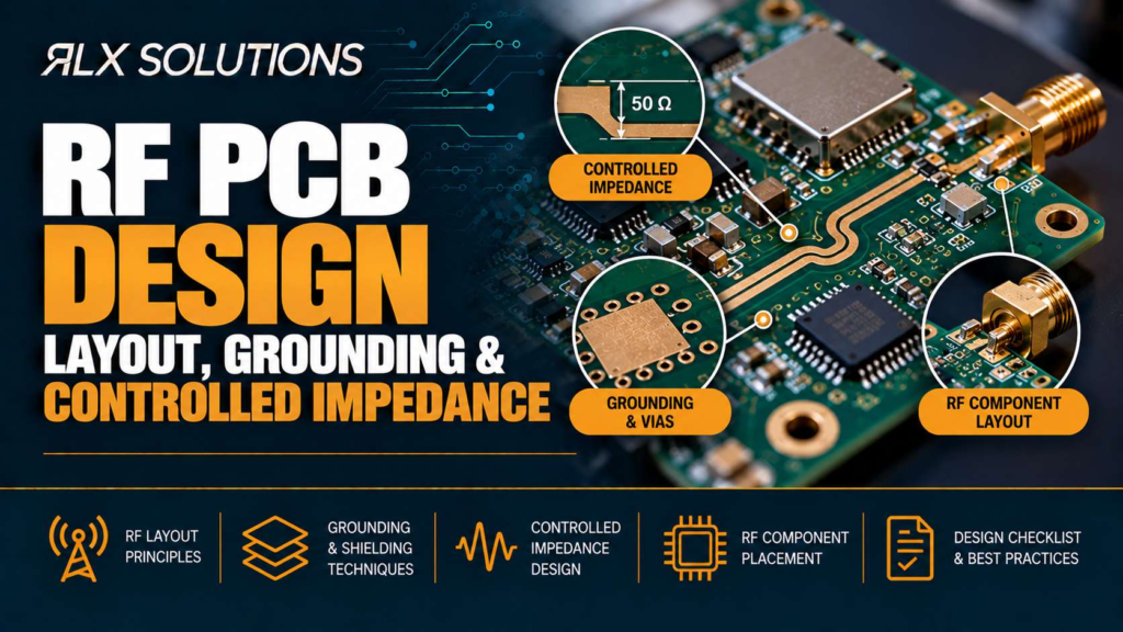
PCB engineering turns schematic intent into a printed circuit board that can be fabricated,
assembled, tested and operated without electrical or thermal surprises. RLX Solutions, a
contract electronics manufacturer in Concord, Ontario, approaches layout as one connected
problem: stackup, routing, manufacturability, signal return paths, heat flow and release
documentation all have to agree.
Set PCB constraints before placing components
The highest-value PCB layout decisions happen before placement begins. Board outline,
connector positions, stackup, copper weight, impedance targets, high-current paths,
thermal limits and assembly requirements define the physical problem the layout must solve.
A useful constraint set covers five areas:
-
Mechanical: board outline, mounting holes, keepouts, connectors,
enclosure interfaces and component height limits. -
Electrical: controlled-impedance nets, differential pairs,
high-current rails, voltage-clearance requirements and sensitive analog nodes. -
Fabrication: layer count, copper weight, trace and space,
drill geometry, via structures, solder mask and surface finish. -
Assembly: package pitch, component orientation, access for inspection,
rework constraints and through-hole requirements. -
Verification: signal integrity (SI), power integrity (PI),
thermal analysis, electromagnetic interference and compatibility (EMI/EMC),
and production test strategy.
The reason for defining these together is simple: changing one constraint can move several
others.
Reducing board area, for example, can force denser routing. Denser routing may require blind
vias or microvias. Those structures can change the lamination sequence and fabrication cost.
A new signal-layer assignment can then change impedance geometry and reference planes.
Treat the stackup and layout rules as engineering inputs, not cleanup tasks.
Build the PCB stackup around return paths
A layer stackup is the ordered arrangement of copper and dielectric layers that determines
routing space, reference-plane geometry, impedance behaviour and part of the board’s thermal
path.
Start by deciding which signal layers require an adjacent continuous reference plane.
High-speed traces should not be routed first and assigned a reference later. Their
electromagnetic fields exist between the trace and its reference structure, so the
reference is part of the interconnect.
For an eight-layer board, a conceptual arrangement might look like this:
| Layer | Possible role | Engineering reason |
|---|---|---|
| Layer 1 | Components and critical signals | Direct access to components |
| Layer 2 | Ground plane | Close reference for Layer 1 |
| Layer 3 | Internal signals | Controlled routing channel |
| Layer 4 | Power or ground | Plane structure and power distribution |
| Layer 5 | Power or ground | Plane structure and power distribution |
| Layer 6 | Internal signals | Additional controlled routing |
| Layer 7 | Ground plane | Reference for Layer 8 |
| Layer 8 | Components and signals | Bottom-side placement and routing |
This is not a universal eight-layer recipe. Dielectric thickness, copper thickness,
impedance targets and power-distribution requirements determine the final construction.
Controlled impedance is a manufacturing specification as well as a layout constraint.
The fabricator needs the target impedance, layer, copper geometry and stackup context
because final trace geometry depends on the actual laminate construction. Controlled
impedance can be produced to ±10% and verified by time-domain reflectometry (TDR)
on a coupon, with the test report shipped with the order.
Material selection belongs here too. A high-speed link should not be assigned a generic
dielectric constant copied from an unrelated stackup. If loss, frequency or channel length
makes laminate properties significant, select the actual material family and model the
interconnect using its applicable electrical data.
Component placement controls more than routing density
Placement sets the geometry of signal loops, power paths, heat flow and assembly access.
Routing can refine good placement, but it rarely repairs poor placement without compromise.
Place mechanically fixed items first. Connectors, switches, displays, mounting hardware
and enclosure interfaces often have little freedom later.
Then place components according to electrical relationships. A switching regulator,
its input capacitor, switching node, inductor and output capacitor form a power-conversion
loop. Spreading those components across convenient empty board space increases loop area
and parasitic inductance even if the ratsnest still connects correctly.
For digital systems, locate processors, memory and high-speed interfaces according to the
channels between them. Decoupling networks need short current paths to the relevant power
and ground structures. Sensitive analog circuitry should be located with awareness of
switching nodes and return currents rather than separated by arbitrary visual zones.
Thermal placement has a similar cause-and-effect chain. Moving two hot devices beside
each other may simplify routing but concentrate heat into the same copper and airflow
region. Moving a temperature-sensitive analog circuit beside a regulator can expose it
to both conducted heat and switching noise.
Placement therefore needs to be reviewed electrically, thermally and mechanically before
dense routing locks it in.
Route for signal integrity, not visual symmetry
Signal integrity is the preservation of an electrical waveform as it moves through an
interconnect. On a high-speed PCB, a trace is part of an electromagnetic transmission
structure, not simply a copper connection between two pins.
Where does the signal current travel?
The outgoing conductor is visible in CAD. The high-frequency return current is less
visible, but just as important. It follows the lowest-impedance return path, usually
concentrated near the signal trace on its reference plane.
A trace crossing a split or void in that plane forces the return current to take a longer
path. Loop area increases, which can raise inductance and radiated emissions.
What happens at each geometry change?
Trace-width changes, connectors, pads, vias and layer transitions introduce impedance
discontinuities. A single small discontinuity may be tolerable. A long channel containing
many poorly controlled transitions can consume the available signal margin.
What couples into nearby structures?
Electric and magnetic fields can couple energy between neighbouring routes. Longer
parallel runs increase the opportunity for crosstalk. Spacing, reference-plane proximity
and routing-layer selection therefore work together.
Worked example: an eight-layer high-speed interface
Consider an eight-layer, 1.2 mm hypothetical circuit board with a differential pair routed
on Layer 1 over a Layer 2 ground plane. The pair changes layers near a connector and
continues on Layer 3.
If Layer 3 references a different plane, the transition is more than two signal vias.
The return current also needs a short path between the two reference structures. Ignoring
that transition can create a larger current loop exactly where the signal already encounters
via discontinuities.
Keeping the pair on Layer 1 for a few extra centimetres may look less direct in CAD,
yet it can be electrically cleaner if it avoids an unnecessary layer change. The shortest
geometric route is not automatically the lowest-risk signal path.
This is why stackup engineering and SI review need to happen before final routing density
leaves no alternatives.
DFM is a release gate, not a design-rule check
Design for manufacturability (DFM) evaluates whether the CAD geometry can be produced
repeatably by the intended fabrication and assembly processes. A design-rule check finds
violations against rules entered into the CAD system. It cannot tell you whether those
rules describe the manufacturing process you actually intend to buy.
Copper weight is one example.
For a two-layer rigid board using 1 oz outer copper, 3 mil trace and 3 mil spacing can be
supported. Move the same design to 2 oz copper and the applicable trace and spacing move
to 6 mil / 6 mil. The electrical schematic has not changed, but the etching problem has.
Via geometry creates another interaction. Mechanical plated through-holes can start at
a 0.15 mm drill, but hole diameter cannot be selected independently of finished board
thickness because the plating process also has an aspect-ratio constraint.
Worked example: drill diameter versus board thickness
Take a hypothetical 1.6 mm thick board.
With a 0.15 mm mechanical drill:
Aspect ratio = 1.6 / 0.15 = 10.67:1
That exceeds a 10:1 standard aspect ratio.
Change the drill to 0.20 mm:
Aspect ratio = 1.6 / 0.20 = 8:1
The second geometry gives the plating process more room without changing layer count or
board thickness.
A designer who checks only the minimum drill size could therefore create a geometry that
looks individually valid but becomes problematic when combined with board thickness.
Annular ring needs the same system-level treatment. The available fabrication geometry
supports a 0.075 mm minimum inner-layer annular ring and 0.1 mm on outer layers.
Pad diameter, drill tolerance, registration and breakout risk all meet at that feature.
Engineer-reviewed DFM needs to evaluate the combination, not isolated minimums.
Same layer count can hide very different manufacturing processes
Two printed circuit boards with ten layers can require very different fabrication routes.
Layer count is therefore a weak proxy for manufacturing difficulty.
Consider these hypothetical designs:
| Decision factor | Board A | Board B |
|---|---|---|
| Layer count | 10 layers | 10 layers |
| Thickness | 1.6 mm | 1.6 mm |
| Main via type | Through vias | Microvias plus buried vias |
| Laser structures | None | Layer 1 to 2 and Layer 2 to 3 |
| Internal structure | No buried-via requirement | Layer 3 to Layer 8 buried vias |
| Fine-pitch escape | Conventional fanout | Via-in-pad under 0.4 mm pitch BGA |
| Filled/capped pads | Not required | Resin-filled, copper-capped and planarized |
| Lamination | Conventional multilayer build | Sequential lamination required |
Board A can drill its through vias after the multilayer structure is assembled.
Board B cannot follow the same sequence. Its buried vias must be created in the relevant
internal subassembly, while blind structures require access to specific layer pairs.
Laser-drilled microvias introduce another drilling and plating operation. Via-in-pad also
adds fill, copper cap and planarization when the pad needs to remain flat for component
attachment.
The result is more manufacturing stages despite identical layer count.
That difference matters during layout because an avoidable via architecture can impose
process steps across the whole board. A 0.4 mm pitch BGA may genuinely justify a dense
fanout scheme. Using the same structure for low-density circuitry elsewhere simply because
it is available does not.
Blind vias, buried vias, stacked or staggered microvias and plated-over filled vias should
therefore be defined as part of the stackup architecture rather than added one net at a
time during final routing.
Give heat a complete path out of the component
Thermal design is the control of heat generation, conduction, spreading and removal so
component temperatures remain within the intended operating limits.
A large copper pour alone is not a thermal strategy. Heat has to travel from the
semiconductor junction through the package, into board copper and vias, through any
interface or heat sink, and finally into the surrounding environment.
Every interface contributes thermal resistance.
That makes layout geometry important. Thermal vias can move heat between copper layers,
internal planes can spread it laterally, and component placement can prevent one heat
source from pre-heating another.
Worked example: a six-layer power board
Consider a hypothetical six-layer, 1.6 mm circuit board using 2 oz outer copper.
A power device dissipates 6 W through an exposed thermal pad.
One layout connects that pad to a top-layer copper region but places no conductive path
to the internal and bottom copper.
A second layout uses the same top copper area but adds twelve 0.30 mm plated vias beneath
and around the thermal pad. At 1.6 mm board thickness, each via has an approximate aspect
ratio of:
1.6 / 0.30 = 5.3:1
The second layout creates parallel conductive paths into additional copper layers.
It does not guarantee a particular component temperature because airflow, package
resistance, copper geometry, dielectric construction and enclosure conditions still
matter. It does, however, create a physically different route for heat to leave the
component.
Thermal vias also interact with assembly. Open vias inside a solderable thermal pad can
affect solder behaviour. If via-in-pad is required, resin filling, copper capping and
planarization allow the pad surface to be restored before assembly.
That is a clear example of thermal engineering triggering a fabrication decision.
Surface finish, solder mask and assembly choices belong in PCB engineering
The bare board is designed for a later assembly process, so pad finish and mask geometry
need to match the component and soldering plan.
Electroless nickel immersion gold (ENIG) provides a flat solderable surface and is useful
where fine-pitch pad coplanarity matters. Electroless nickel electroless palladium
immersion gold (ENEPIG) is available where requirements such as wire bonding drive the
finish selection. Organic solderability preservative (OSP) can be used for single-reflow
builds in this manufacturing flow.
Gold fingers are a different case. They are contact surfaces rather than ordinary solder
pads, so hard gold and edge bevel requirements need to be called out explicitly.
Solder mask geometry can also decide whether a dense footprint is manufacturable.
A 0.08 mm mask dam can be produced between pads, with 0.05 mm per-side expansion as the
default. On dense packages, the engineer should confirm whether the preferred mask-defined
or copper-defined geometry actually leaves enough manufacturable mask between adjacent
features.
Finish should therefore be selected from the assembly and product requirements, not from
habit at the end of CAD release.
Design inspection and test access into the layout
A board that cannot be inspected or tested efficiently can create production problems even
when its electrical design is sound.
For assembled boards, inspection can include 100% solder paste inspection before reflow,
automated optical inspection after reflow on both sides, and X-ray inspection for
structures such as ball grid arrays (BGAs), land grid arrays (LGAs) and quad flat no-lead
(QFN) thermal pads.
The layout affects how useful those methods are.
Functional test access, programming headers, ground points and probe targets should be
allocated before the remaining free space disappears. Flying-probe in-circuit test can
provide full-net coverage for prototype and low-volume work without a dedicated fixture.
Production volumes can use bed-of-nails in-circuit testing where a fixture is appropriate.
If the product requires functional test, define pass/fail behaviour and the interfaces
needed to exercise it. Functional test can then be logged with serial traceability rather
than becoming an improvised bench procedure after assembly.
Build class matters as well. IPC-A-610 Class 2 and Class 3 workmanship requirements affect
inspection and acceptance, while IPC-6012 Class 2 and Class 3 apply to bare-board
fabrication. Class 3 involves tighter fabrication and workmanship expectations, so the
intended class should be established before the package is released.
Release manufacturing data as one controlled package
The fabrication package needs to describe the board without forcing the manufacturer to
infer design intent.
Manufacturing outputs can be supplied as Gerber RS-274X, ODB++ or IPC-2581 together with
NC drill data. The supporting documentation should carry the information that artwork
alone cannot express clearly.
A complete release can include:
- Stackup drawing or PDF with layer order and board construction intent.
- Controlled-impedance targets and the nets or classes they apply to.
- Fabrication notes covering material, copper, finish and special processes.
- Clear identification of plated and non-plated holes, slots and cutouts.
- Assembly drawing and polarity or orientation information.
- Bill of materials in .xlsx or .csv format.
- Pick-and-place or centroid file.
- Test, programming and serialization requirements where applicable.
Native design data is also useful when an engineering review requires more than
manufacturing artwork. Altium, Eagle, KiCad, OrCAD and DipTrace design files can be
handled alongside the manufacturing package.
The important distinction is between geometry and intent. Gerber data can show where
copper exists. It does not, by itself, explain why a differential pair needs an impedance
target, whether a connector finger requires hard gold, or whether a buried via is
intentional.
A controlled release should make those decisions explicit.
Make the engineering handoff reviewable
If a board is approaching prototype or production release, RLX Solutions can review
schematic, layout, stackup, SI/PI, thermal considerations and DFM/DFA as part of the
engineering and manufacturing handoff. Engineer-reviewed DFM/DFA is included on every
quote, so fabrication constraints can be addressed before manufacturing data becomes a
purchase-order problem.
PCB Engineering Guides in This Series
Each guide below covers one part of PCB engineering in more depth, grouped by topic.
Design Fundamentals
- PCB Layout Design: Complete Guide to Placement, Routing & Manufacturability
- PCB Schematic Design: From Circuit Diagram to Layout
- PCB Component Placement Guidelines
DFM & Design Review
- PCB Design Review Checklist Before Production
- DFM vs DFA in PCB Design & Assembly
- PCB Design for Manufacturing: Complete DFM Guide
RF & Analog
- RF PCB Design: Layout, Grounding & Controlled Impedance
- Mixed-Signal PCB Design: Analog & Digital Layout Guidelines
High-Speed & Signal Integrity
- High-Speed PCB Design: Stackup, Routing & Signal Integrity
- Differential Pair Routing: Impedance, Spacing & Length Matching
- Signal Integrity in PCB Design: Routing, Impedance & Return Paths
- PCB Crosstalk: Causes, Effects & Layout Fixes
- PCB Length Matching: When Trace Length Matters
- BGA Fanout & Escape Routing: Vias, Layers & Routing Strategies
Thermal Engineering
- Thermal Vias in PCB Design: Size, Spacing & Placement
- PCB Thermal Management: Heat Dissipation, Copper & Vias
Flex & Rigid-Flex
High Voltage
Power & Grounding
- PCB Ground Plane Design: Grounding Rules & Common Mistakes
- Power Integrity in PCB Design
- Decoupling Capacitor Placement for PCB Power Integrity
- PCB Power Distribution Network Design
EMI & EMC
Standards & Compliance
Related guides: PCB Manufacturing Guide, PCB Assembly Guide and PCB Applications by Industry.
Frequently Asked Questions
When should I use microvias instead of mechanical through vias?
Use microvias when package density or escape routing cannot be solved efficiently with
through-hole geometry. A 0.10 mm laser-drilled microvia can support dense structures,
including stacked and staggered arrangements, but it also changes the fabrication
sequence. Confirm layer pairs, stacking strategy, fill requirements and sequential
lamination before completing fanout.
How should controlled impedance be documented for fabrication?
Identify the target impedance, relevant nets or net classes, routing layer and intended
stackup rather than specifying trace width alone. The final geometry is connected to
copper thickness and dielectric construction. Controlled impedance can be verified to
±10% using a TDR coupon, with the resulting test report supplied with the order.
Does a 0.15 mm minimum drill mean I can use it on every board thickness?
No. Minimum drill diameter is only one part of via feasibility. Board thickness divided
by hole diameter determines the aspect ratio, which affects the plating process.
A 0.15 mm drill through a 1.6 mm board produces roughly a 10.67:1 ratio, so a larger
drill or different via architecture may be needed.
What is the difference between IPC-6012 and IPC-A-610 in a PCB programme?
IPC-6012 applies to rigid printed circuit board fabrication, while IPC-A-610 covers
acceptance of assembled electronic hardware. A programme can therefore have requirements
at both stages. If Class 3 is specified, that decision affects fabrication, assembly
workmanship, inspection and documentation rather than being a label added after
production.
Can PCB engineering include signal integrity and thermal review before layout is complete?
Yes. Early review is often more useful because the stackup, layer assignment, placement
and via architecture can still change. Requirements capture, stackup and impedance
engineering, high-speed digital layout, power-delivery design, thermal analysis and
EMI/EMC design review can be addressed before fabrication files are released.